

As always, I am amazed by the astounding ingenuity of the human race, of which I am proud to be a card-carrying member. The reason I say this is that my eyes were just opened to a profusion of production possibilities provided by a revolutionary new ultra-high resolution 3D printing technology that could transfigure and transform a wide range of industries, including semiconductor and display manufacturing.
In a recent column — Welcome to a World of Reconfigurable Intelligent Surfaces — I made mention of the fact that: “Some people tend to talk in terms of ‘ages,’ like the stone age, the bronze age, the iron age, and the industrial age. Others talk about the pre-mechanical age, the mechanical age, the electromechanical age, and the electronic age. Some may talk about the computer age, the data age, or the information age. Personally, I am convinced that we will soon crack the door open into what I call the materials age, as part of which we will have the ability to ‘print’ new materials atom by atom on an industrial scale.” Well, we aren’t there yet, but the news I am poised to impart certainly takes us one giant step closer.
This all started when I saw a press release about a Swiss company called Scrona AG receiving millions of dollars in funding. Generally speaking, I pay little attention to the business side of things because I’m interested only when a company has a cool technology. This is certainly a cool technology. What really caught my eye in the aforementioned press release was the part where Scrona’s co-founder and CEO, Dr. Patrick Galliker, made the comment: “Scrona is enabling customers to digitally print the impossible, on any material, at scale […]” Like most engineers, I’m an adherent to the saying, “The impossible we do at once; miracles take a little longer,” so I determined to discover more, and it wasn’t long before I was having a video conference with Patrick and Walter Braun, who is Scrona’s COO.
Before we proceed, I would like to go on the record as saying that I’m tremendously impressed with today’s inkjet printers, which perform their magic by spraying liquid ink through microscopic nozzles. You have to remember that my early career involved my working with ASR 33 Teletype terminals, like the one sitting in the corner of my office. These little beauties, which used continuous (fan-fold) paper, could print only alphanumeric and punctuation characters — 72 characters a line at 10 characters per inch. Even with these limitations, I remember people creating extraordinary complex (on occasion, outrageously large) images in the form of ASCII art, which can look amazing when seen from a distance or if you squint your eyes when looking up-close.
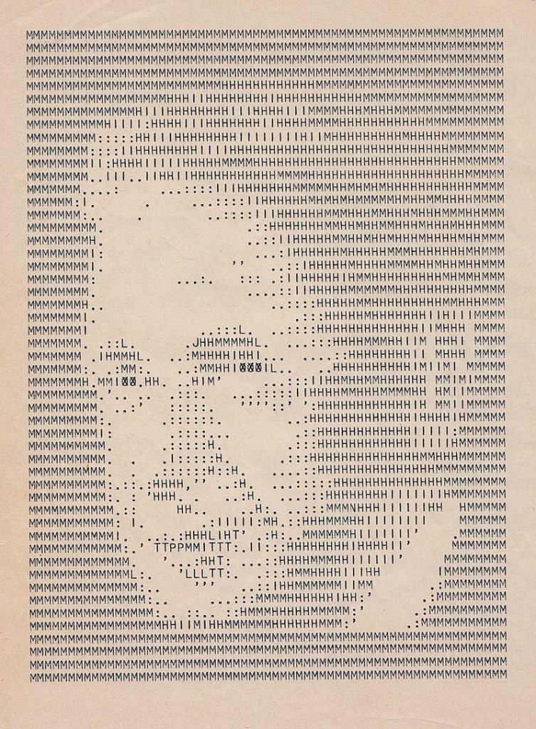
Dag Hammarskjöld, printout from teleprinter 1961-62
(Image source: Jonn Leffmann/Wikipedia)
I remember when ASCII art was state-of-the-art with respect to the sort of imagery most of us engineering grunts could hope to create. Now, of course, we have the aforementioned inkjet printers that allow us to create high-resolution images in glorious technicolor, but just how high resolution are we talking about, what are the limitations with regard to 3D printing and additive manufacturing, and what are the alternatives? I’m glad you asked. Take a look at the image below comparing piezo-based inkjet technology versus Scrona’s NanoDrip technology.
Comparison of piezo-based inkjet technology (left) vs. Scrona NanoDrip technology (right) (Image source: Scrona)
Now, I’m sure you would take exception to someone calling you any sort of drip, but I think I can persuade you that the coolest and sexiest form of drip is a NanoDrip. As we will discuss, when it comes to using printing technology to create electronic systems and displays, it all comes down to how the drops are created and how small you can coerce the little rascals to be.
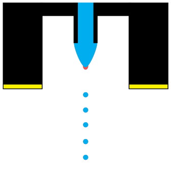
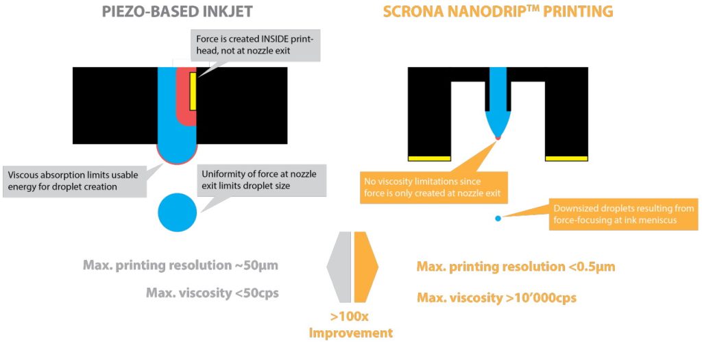
I’m afraid that it’s a tad tricky to read the text in the above diagram, but I’ll do my best to explain what’s going on. Let’s start with the piezo-based inkjet on the left. This uses a push mechanism to expel the drops of ink (shown in blue) out of fine microfluidic structures we could call nozzles. Inside each nozzle we have the piezo element (shown in yellow) that creates the pressure. Squeezing a piezoelectric material causes it to generate an electric potential. Contra wise, applying an electrical potential to a piezoelectric material causes it to deform, generating a pressure wave in this case — a pulse of pressure if you will — that propagates through the ink.
The ink itself is essentially part of the “mechanical” system. The bulk of the pressure (the large red area) surrounds the piezo element. The ink’s resistance to the pressure wave from whence it’s created to where it’s needed at the end of the nozzle consumes a lot of energy and creates a limitation as to how small we can go in terms of nozzle diameter. A related point is that an inkjet printer by design has a very narrow window of (generally very low) viscosity it can work with, which limits the inks we can use. Relatively little energy makes its way to the edge of the ink (the thin red line at the edge of the ink). At this point, the force is uniformly distributed, with the result that the ensuing droplet is approximately the same diameter as the nozzle.
Now, let’s turn our attention to Scrona’s NanoDrip technology. Once again, the force generators are colored yellow. In this case, however, these force generators, which are electrostatic in nature, are located outside of the nozzle. These little scamps generate an electrostatic field that pulls the ink (blue) out of the nozzle, thereby facilitating the use of higher-viscosity inks. Furthermore, the force accumulates and is expressed at the very tip of the ink, which becomes the actuation element, resulting in much smaller droplets than can be achieved by conventional inkjets.
The result is >100% improvement in both resolution and viscosity. For example, an inkjet supports a maximum resolution of ~50µm, while NanoDrip technology offers <0.5µm (I’m informed that 0.05µm can be achieved in principle). In the case of viscosity, we can cover a range that spans the equivalent of water (regular inks) to honey. In turn, this means that NanoDrip printheads can work with all of the specialist inks from hundreds of suppliers that are currently commercially available on the market, including inks with metallic properties, inks with insulating properties, and inks with semiconducting properties — basically anything we need to create an electronic product in the form of circuits and displays.
In addition to ultra-high-resolution printing (100X higher than inkjets), this technology supports high-speed printing because smaller droplets dry faster resulting in 10X throughput per printhead area, with respect to which we can be talking about 1,000 or more nozzles per printhead. Also of interest is the fact that this technology supports 3D printing with aspect ratios of >10:1 coupled with nanometer thickness control, which means we can increase the conductivity of tracks without consuming additional real-estate on the substrate, for example.
Scrona’s NanoDrip technology flings open the doors to an incredible array of addressable markets and applications — semiconductors, PCBs and printed electronics, MEMS and sensors, displays and touch sensors, etc. — enabling the production of completely new products whilst disrupting existing wasteful manufacturing processes. Take today’s System-in-Package (SiP) modules, for example, in which multiple chiplets (silicon dice) are mounted on a common substrate. The equipment used to implement the substrate can cost tens of millions of dollars. Creating a single redistribution layer (RDL) on the substrate can require as many as 22 steps that are wasteful of expensive and/or toxic materials. By comparison, creating an equivalent product employing additive manufacturing using Scrona’s NanoDrip printheads requires only two steps, thereby slashing CAPEX (capital expenditures) by 10X and OPEX (operating expenses) by 5X.
Until now, it’s been possible to state with some certainty that competitive additive manufacturing in this arena has been either precise or fast but not both. Well, it’s time to perform our happy dance because — as illustrated in the diagram below — Scrona’s multi-nozzle printheads fulfill stringent precision and resolution requirements while scaling to mass-production throughput.
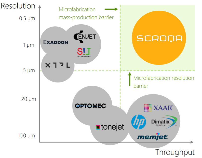
The NanoDrip competitive advantage (Image source: Scrona)
One point I find really interesting is that the guys and gals at Scrona don’t want to build everything themselves — they are happy to focus on developing the latest and greatest in printhead technology and to have their printheads incorporated in other companies’ products, thereby allowing them to overcome the high barriers to entry into different markets. The folks at Scrona are already working to create standardized industrial printheads with leading equipment manufacturers like Notion Systems, and they are also engaged in feasibility studies with Tier 1 leaders in digital print, semiconductor, and display devices.
I for one am very impressed. My head is currently buzzing with ideas for NanoDrip applications (and that’s not something you expect to hear yourself say every day). I’m assuming that the term NanoDrip meant nothing to you before you started reading this column. I hope you’ll now agree with me that this is the day the NanoDrip moniker became sexy.


