

Last week, Synopsys invited a handful of journalists and analysts to attend their annual SNUG (Synopsys Users’ Group) meeting for the first time in 30 years. Why? What message did the company want to get out that was important enough to allow the foxes into the henhouse, to breach the traditional sanctity of the tight company-user relationship that has been guarded at these events for the last three decades?
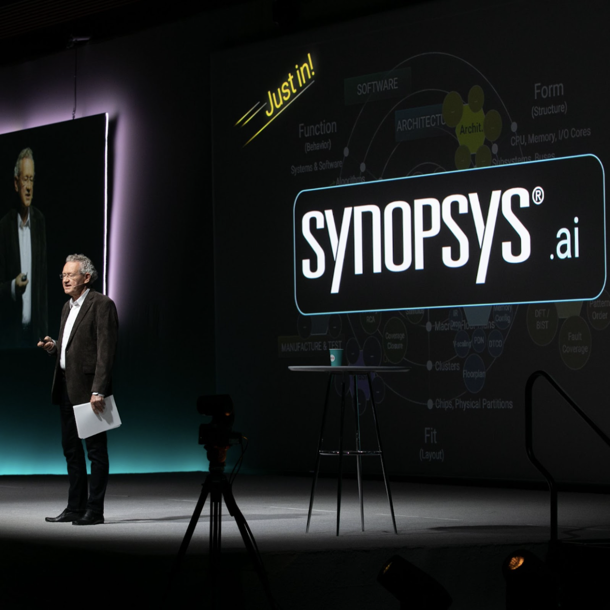
The headline SNUG 2023 announcement is Synopsys.ai – an all-encompassing adoption of AI technology into the entire EDA ecosystem, from design, verification, and IP through manufacturing and test. Just about every part of the Synopsys IC design solution stack has been wrapped in, or infused with, AI and machine-learning technology. Obviously, that’s a big deal. But big enough? After all, everyone is wrapping AI around everything these days.
While there has been a lot of hubbub the last few months about general-purpose generative AI being able to perform party tricks like writing simple Verilog code, the real applications of AI in EDA are much more complex and subtle. General purpose AI doesn’t work for highly domain-specific tasks such as chip design, because the data required to successfully design leading-edge semiconductor devices isn’t available in any training model. That information is generally part of enormous collections of well-kept secret tricks and techniques buried in various tech companies and in the heads of their key design talent.
Synopsys has taken this challenge head on and come up with solutions that are both powerful and practical. The three major components of Synopsys.ai are DSO.ai, VSO.ai, and TSO.ai – aimed at design space optimization, verification space optimization, and test space optimization, respectively.
DSO.ai – Digital design space optimization works autonomously to achieve power, performance and area (PPA) targets using intelligent massively-scaled application of Synopsys design tools. The skill and experience required to take maximum advantage of modern EDA technology is daunting. The tools and design flows have become so complex, and the design constraints and targets so varied that a team of experts is generally required to get a design to fit within the tight multi-constraint target windows. DSO.ai searches for optimization targets in the impossibly large solution spaces of chip design to find candidate solutions that deliver against key PPA design metrics. While doing so, it utilizes “reinforcement learning” to create improved results for future designs. Some customers report large frequency improvements (up to 100MHz), significant power reduction (15%), and 3x productivity enhancements – taking weeks off their product development times. At the time of SNUG, Synopsys says DSO.ai has been used in over 160 tape-outs.
While on the topic of reinforcement learning, it’s important to point out that Synopsys has a very clean and straightforward solution to preserving proprietary design expertise while maximizing the contribution of AI models for each company. To put it simply, your company’s AI models are created based on experience with your company’s designs, with the results of this learning kept secure and separate for each company.
VSO.ai – Verification Space Optimization uses similar AI-driven exploration to achieve coverage closure faster and with higher quality. The company says, “The system works autonomously to reach coverage targets as quickly and as cheaply as possible with higher quality of results. Machine learning technologies are used to identify and eliminate redundancies in regressions, automate coverage root cause analysis, and infer coverage from RTL and stimulus to identify coverage gaps and provide coverage guidance.” One customer reports a 10x acceleration in deep bug hunting and coverage closure with a net 30% increase in overall IP verification productivity.
Synopsys TSO.ai uses AI to minimize test cost and time-to-market by automatically searching for an optimal solution in a large test search space, working to minimize pattern count. The company showed impressive results in the system’s ability to automatically discover test pattern solutions that were considerably better than conventionally designed test programs in a fraction of the time.
Clearly this technology works, and the customer-level buzz on it was substantial. And, when combined with the other tea leaves that are dropping as if we were in an early-autumn freeze, we see an inflection point in the industry, a new era of EDA and of electronic technology itself.
That is most certainly a big deal.
This new age of EDA is sparked by a confluence of simultaneous discontinuities – the economic demise of the traditional notion of Moore’s Law, the ascent of artificial intelligence, and the rapid adoption and progress in multi-die system-in-package technology.
In his keynote, Synopsys CEO Aart de Geus was quick to point out that Moore’s Law has not ended. Semiconductor companies will continue to shrink transistors for at least another decade. But that has already started to yield drastically diminishing returns. No longer does the next node give us double everything – performance, power efficiency, and density. In fact, we are lucky to get modest increments in two out of three key metrics.
Instead, the spirit of exponential technological progress has simply shifted and evolved. Where the letter of Moore’s Law was about “Cramming More Components onto Integrated Circuits” – meaning increasing the number of transistors on a chip by a factor of two every couple years – the result, the reason Moore’s Law mattered – was long-term exponential improvement in the capabilities of the technology that we produce.
Every two years, cool technology stuff got faster, cheaper, more capable, and used less power.
We’ve enjoyed this progress – the bounty reaped from packing more transistors onto chips – for the past sixty years. De Geus argues that we will continue to see that rate of technological progress, but the driving forces behind that momentum will be much more diverse and complex. He calls this new trend “SysMoore” – meaning exponential improvement in technology’s capabilities at the system level, driven by countless collaborative innovations – not just increasing numbers of transistors.
SysMoore relies on innovation in architecture, packaging, and engineering productivity to augment the traditional process-based gains. Essentially, it picks up the slack where traditional Moore’s Law is waning with fresh engineering across a wide swath of disciplines.
At the same time as AI-driven design optimization is moving into prominence and Moore’s Law is morphing, we have reached a critical point in the development evolution of multi-chip system design and implementation. We will be seeing increased use, and ultimately widespread adoption of chiplet-based design with advanced packaging techniques. This will tame problems currently associated with high-end PCBs – interconnect density, bandwidth, signal integrity, power consumption, integration of diverse chips fabricated in different processes from different manufacturers – unicorns, rainbows – everything will be bliss in multi-chiplet land.
In effect, it’s a bright new day for engineers. Because, while Moore’s Law gave us a shiny new 2x of awesomeness every 24 months or so, it was also a ruthless taskmaster. Massive amounts of engineering talent and effort were required just to get our existing designs and tools ready for the next node. The tyranny of the shrink consumed vast resources and left little time for other innovation. Why burn brain time coming up with a trick that will improve your design by fifteen or twenty percent, when being the first on the next process node gives you a guaranteed 2x?
Now, we have a whole new playing field, where multi-disciplined innovation will drive progress forward – where engineers will be freed from the oppression of the Moore’s Law curve and empowered to bring their best and most creative ideas to the table… If only we had enough engineers.
That’s where the productivity element comes in, and that’s why EDA is poised to occupy an even more central role than ever – giving engineers power tools for innovation, allowing them to create larger, more complex, more capable designs than ever before, and focusing on true innovation rather than turning the crank on yet another node shrink.


