

Many of today’s electronic systems feature multiple printed circuit boards (PCBs) and/or modules. (For the remainder of this column, unless such interpretation is inconsistent with the context, we will assume the term “board” to embrace the term “module.”) Not surprisingly, the system’s designers often wish to pass data back and forth from board to board.
Oftentimes, these inter-board signals involve relatively low-speed data transfer via general-purpose input/output (GPIO) pins or low-bandwidth serial interfaces like I2C (inter-integrated circuit) and I2S (integrated inter-IC sound bus).
One solution is to use rigid-flex boards, which are hybrids between traditional rigid PCBs and flexible printed circuits (a.k.a. flex circuits), where the latter consist of a thin insulating polymer film with conductive traces printed on one or both sides (an additional thin polymer coating is subsequently applied to protect the conductive traces).
Unfortunately, rigid-flex boards are significantly more expensive than regular boards (see also Why is Rigid-Flex So Expensive?). Also, rigid-flex isn’t an option if the various boards are coming from multiple vendors. Furthermore, even if all of the boards are being manufactured by the same company, one problem with rigid-flex is that the boards are permanently connected together (the flex enters the rigid boards as a layer in the middle). Now, you might be saying “Duh! Isn’t that the point?” But when you come to think about it, you realize that this means you are SOL (sort-of out of luck) if you wish to replace or upgrade one or more of the boards while leaving the rest of the system intact.
Another common option is to mount multi-pin connectors on the boards and then use multi-wire harnesses to connect the boards together as illustrated below:
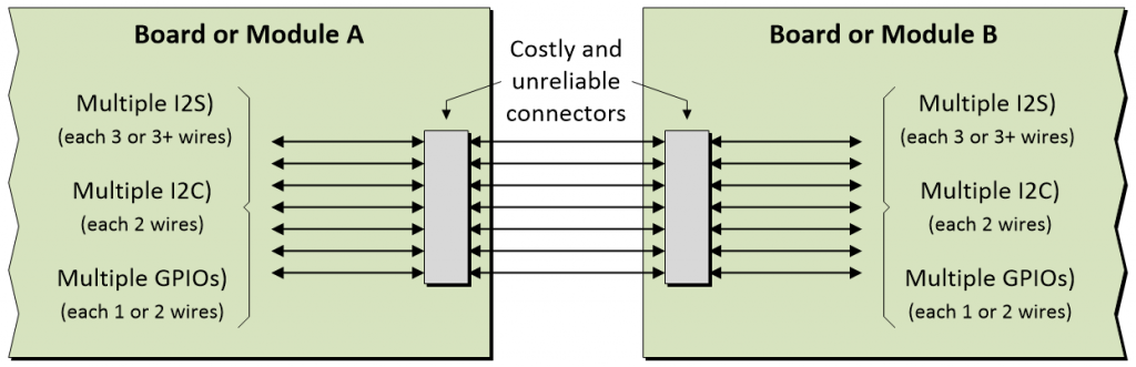
Traditional connectors consume space, cost money, and negatively impact the reliability of the system (Image source: Max Maxfield)
Once again, there are a number of problems with this scenario, including the fact that the connectors consume board real estate and — along with the cables — they increase the cost of the system. Furthermore, each connector pin is a potential point of failure. In fact, connectors are often the overwhelming factor with regard to the reliability, or lack thereof, of the system.
This leads us to another way of looking at things, which is that reducing the number of inter-board connections will lower the cost, decrease the sizes of the boards, and increase the reliability of the system. Well, that sounds easy enough (everything does if you say it quickly), but how are we going to actually do it?
The solution is known as single wire aggregation (SWA). The idea is to take multiple low-bandwidth signals and aggregate them into a higher-bandwidth time division multiplexed (TDM) signal that requires only a single inter-board wire. One way to implement this would be via a custom application-specific integrated circuit (ASIC) as illustrated below:
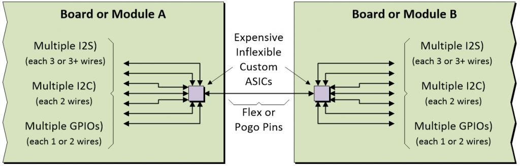
Custom ASICs are expensive, time-consuming to develop, and inflexible (Image source: Max Maxfield)
Of course, this would require a new ASIC design for every project, because once you’ve implemented your algorithms and functions in an ASIC they are effectively “frozen in silicon.” Even worse, creating ASICs is a very expensive, resource-intensive, and time-consuming hobby. As a worse-case scenario, you may have finished all of the board designs and be left waiting for the ASIC to be completed so you can connect the boards together. I know that ASICs are sexy, and you can call me “old-fashioned” if you will, but in this case I think I’ll pass on the ASIC option if you don’t mind.
So, what is our best alternative? Did you say field-programmable gate array (FPGA)? Good Golly Miss Molly, I think you’ve got it! A teeny-tiny FPGA a couple of millimeters square would be just the ticket. In addition to being low-cost and consuming very little power, the programmable nature of an FPGA means that it’s inherently flexible.
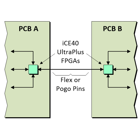
But whose FPGAs should we use? Well, it may not surprise you to hear that those clever folks at Lattice Semiconductor have been looking into SWA, and they’ve come up with a suite of cunning solutions based on their iCE40 UltraPlus FPGAs as illustrated below:
iCE40 UltraPlus FPGAs are small, inexpensive, and flexible (Image source: Max Maxfield)
These little scamps (the iCE4 UltraPlus FPGAS, not the folks at Lattice) boast a flexible logic architecture with 2,800 or 5,280 4-input look-up tables (LUTs), customizable GPIOs, up to 80 kilobits of embedded block memory (EBM), and up to 1 megabit of embedded SRAM. In addition to featuring an ultra-low-power advanced process with static current as low as 75 µA and as little as 1 to 10 mA active current for most applications, iCE40 UltraPlus FPGAs are also available in multiple package options to fit a wide range of applications needs, from an ultra-small 2.15 x 2.50 mm WLCSP package optimized for consumer and IoT devices to a 0.5 mm pitch 7 x 7 mm QFN for cost-optimized applications.
Of particular interest is the fact that the configuration bitstream can be loaded directly into SRAM-based configuration cells, thereby allowing iCE40 UltraPlus FPGAs to be reprogrammed over and over again. This is the best option during the prototyping phase of a project, because it allows you to experiment with different designs and bitstreams.
If the SRAM-based configuration approach is used when the iCE40 UltraPlus is deployed in a product, then the configuration can be loaded via an on-board MCU or from an external SPI Flash memory device. Alternatively, iCE40 UltraPlus FPGAs also contain a one-time programmable (OTP) on-chip non-volatile configuration memory (NVCM), which is best suited for mass production. Once the NVCM has been programmed, the device will automatically, quickly, and securely boot from this configuration.
Now, sit up and pay attention because this is where things start to get very clever indeed. Some teams will include people with FPGA design expertise, while others… won’t. If you have one or more FPGA designers on the team, then Lattice provides some of the easiest-to-use FPGA development tools in the industry. In the case of its SWA solution, Lattice provides source code for an easily modifiable parameterized SWA reference design, an associated SWA Reference Design User Guide, and an SWA demonstration and development board.
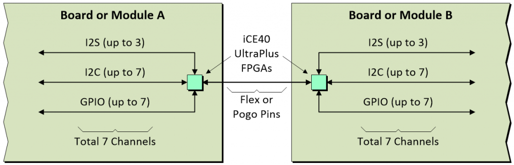
But what happens if you don’t have an FPGA designer on the team? Well, turn that frown upside down into a cheery grin, because the folks at Lattice have you covered. What they’ve done is to analyze multiple real-world products and derive five popular configurations as illustrated below:
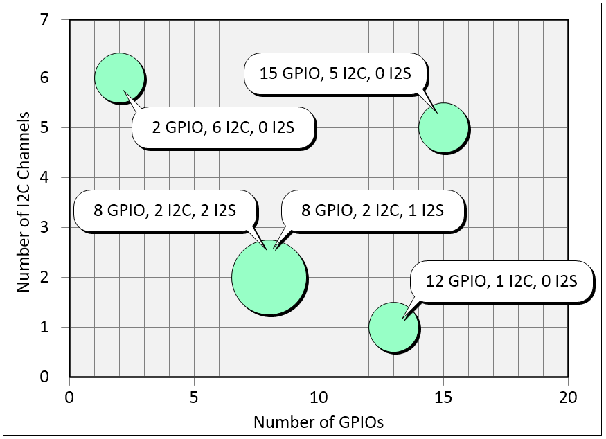
Five popular iCE40 UltraPlus FPGA-based SWA configurations (Image source: Max Maxfield)
They also provide a suite of five pre-synthesized bitstreams associated with these configurations. All you have to do is load the bitstream of choice into your FPGA. How do you do this? Well, put on your “Happy Dance Shoes” because a Bitstream User Guide is available from Lattice’s SWA webpage. This guide describes how anyone can load one of the preconfigured bitstreams into an iCE40 UltraPlus FPGA.
“Ah, ha,” I hear you say (somewhat grumpily, if the truth be told), “but what happens if I don’t have a clue about FPGAs and the five configurations shown above don’t ‘cut the mustard’ with regard to my exceptionally clever design?” Well, aren’t you a little ray of sunshine?
As an aside, if you are a fan of Robert Heinlein, you will doubtless have read The Moon is a Harsh Mistress and be aware of the word “Tanstaafl,” where TANSTAAFL is an acronym for, “There ain’t no such thing as a free lunch.” And, as a “nested aside” (just call me a “programming fool”), the “free lunch” part of this adage derives from the once-common tradition of saloons in the United States providing a “free” lunch to patrons who had purchased at least one drink (the foods on offer were typically high in salt — ham, cheese, and salted crackers — so those who ate them ended up buying more beer). In fact, Rudyard Kipling, writing in 1891, noted how he
…came upon a bar-room full of bad Salon pictures, in which men with hats on the backs of their heads were wolfing food from a counter. It was the institution of the “free lunch” I had struck. You paid for a drink and got as much as you wanted to eat. For something less than a rupee a day a man can feed himself sumptuously in San Francisco, even though he be a bankrupt. Remember this if ever you are stranded in these parts.
But we digress… It seems that TANSTAAFL isn’t always the case, because the guys and gals at Lattice also offer a free SWA design service. If you visit Lattice’s SWA development board webpage, you can use an interactive form to specify the unique combination of channels you require for your design, and the Lattice design team will then email the corresponding bitstream file to you.
To be honest, when I started writing this column, I thought that most of the people I know in embedded space (where no one can hear you scream) would be familiar with the concept of SWA. However, I was involved in a couple of telephone calls while writing, during which I mentioned what I was writing about, and each of my embedded engineering friends said something along the lines of, “Wow! That’s a great idea. Can you email me a link to your column when it goes live?” I certainly can. Furthermore, it would be great if you could email the link to this column to all of your friends and colleagues because they may not know about SWA either, in which case you will be the hero of the hour (try not to let it go to your head). As always, I welcome your comments, questions, and suggestions.


