

There’s an old saying that goes, “Standards are great… everyone should have one.” The problem being, of course, that so many people do, resulting in our being up to our armpits in the little rascals (not that I’m bitter, you understand).
Much the same thing applies to STEM (science, technology, engineering, and math) “laws” — there are now so many of these little scamps, and so many people dropping them willy-nilly into the conversation, that it makes my head spin. For example, I recently received an email saying, “As the cost of semiconductor scaling and innovation continues to rise, Dennard’s law has failed while Moore’s law is at best slowing. This stagnancy is causing the industry to struggle to make major advances in scaling and performance, thereby limiting the advancements for cutting-edge technologies like artificial intelligence (AI) and edge computing.”
I have no idea what drives my mother to send me messages like this, but I wish she would find another hobby. Of course, you’d have to be living under a rock to remain unaware of Moore’s law from 1965, which started off as the observation that the number of transistors we can cram into an integrated circuit (IC) doubles about every two years. To be honest, I was blissfully unaware of Dennard scaling (which some call Dennard’s law), but a quick Google refreshingly revealed that this originated in a 1975 paper in which Dennard observed that transistor dimensions could be scaled by -30% (0.7x) every technology generation, thus reducing their area by 50%.
In turn, this would reduce circuit delays by 30% (0.7x) and therefore increase operating frequency by about 40% (1.4x). Finally, to keep the electric field constant, voltage is reduced by 30%, reducing energy by 65% and power (at 1.4x frequency) by 50%. Thus, the gist of Dennard’s law is that, in every new technology generation, if the transistor density doubles, the circuit becomes 40% faster, and power consumption (with twice the number of transistors) stays the same.
Unfortunately, at the time Dennard co-authored the original paper, leakage was negligible and largely ignored. The problem is that as transistors get smaller and their dielectrics get thinner, they are more prone to leakage. Today, static (leakage) power now approaches the same order of magnitude as dynamic (switching) power. Hence the fact that Dennard’s law is no more (sad face).
And then there’s space (as in rockets and satellites and space probes and spaceships), which introduces all sorts of challenges, not the least of which is radiation, whose effects become more pronounced as the feature sizes on chips shrink.
I love all things space, and I’m tremendously enthused by the possibility of people returning to the Moon and then progressing to Mars. Six years ago as I pen these words, the Philae lander from the European Rosetta space probe performed the first successful landing on a comet. Just one year later, NASA’s New Horizons probe sped past Pluto. Less than a week ago, China successfully landed its Chang’e-5 probe on the surface of the moon with the hope of picking up some lunar material and bringing it back to Earth. And, just a couple of days ago, Japan’s Hayabusa2 space probe actually did return to Earth carrying samples it had picked up from an asteroid named Ryugu.
Also, let us not forget 16 Psyche (it’s hard to get it out of your mind), which — at around 70 miles in diameter — is one of the larger objects in the asteroid belt orbiting between Mars and Jupiter. It now appears that 16 Psyche is largely composed of iron and nickel, making it valuable beyond belief. Did you know that the Colorado School of Mines now offers an advanced degree in asteroid mining? (Well, they call it “Space Resources,” but we all know what they really mean.)
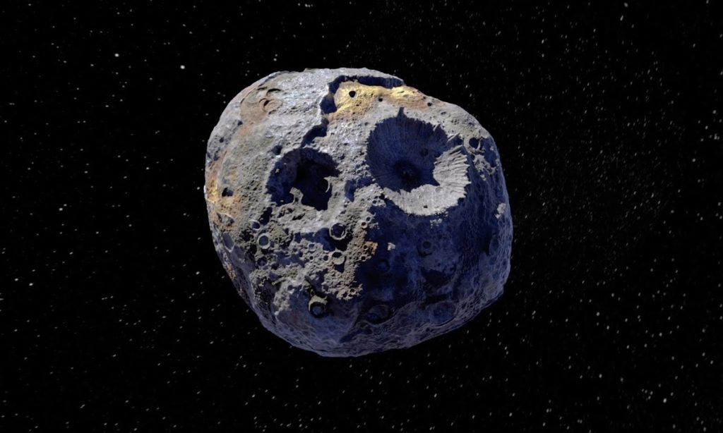
Artistic impression of 16 Psyche (Image source: Maxar/ASU/P.Rubin/NASA/JPL-Caltech)
All of this makes me think of The Rolling Stones (also known as Space Family Stone in the UK) by Robert Heinlein. In this story, a family of “Loonies” (residents of the Moon) called the Stones purchase and rebuild a used spaceship and go sightseeing around the Solar System, including a stop at Mars and a trip to visit the miners in the asteroid belt. I think I’ll re-read this book this evening, but we digress…
One requirement of any electronic system is memory, and today’s applications are demanding more and more of it. Unfortunately, existing non-volatile memory (NVM) technologies like flash (NOR- and NAND-based), along with volatile technologies like SRAM and DRAM, all present a muddled mix of advantages and disadvantages. The ideal solution would be a “universal memory” that was non-volatile like flash, sported the speed of SRAM, and boasted the capacity (density) of DRAM. Oh, yes, and in the case of many applications — especially those bound for space — it should be inherently radiation tolerant for good measure.
A strong contender for the universal memory slot is magnetoresistive random-access memory (MRAM), which was originally developed in the 1980s. As its name suggests, MRAM stores data in magnetic domains and is non-volatile.
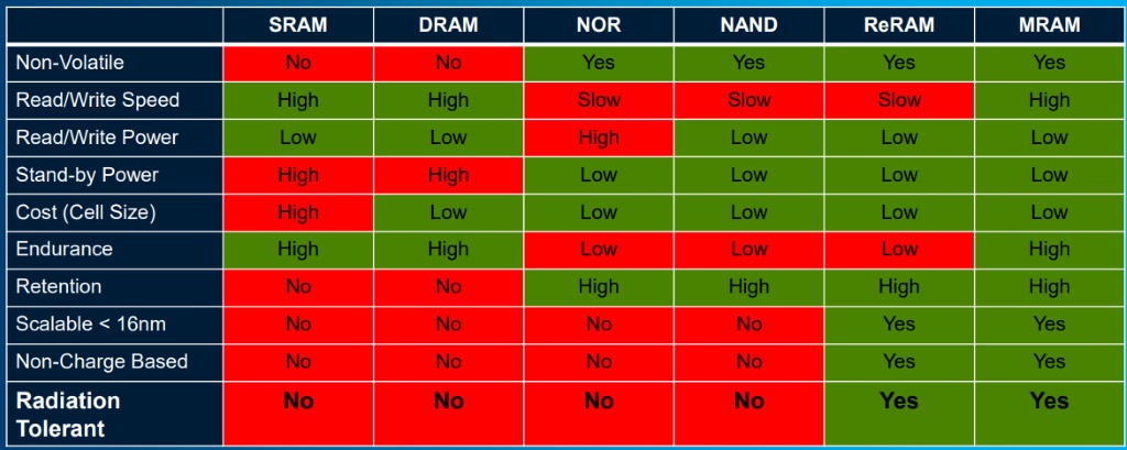
Comparison of different memory technologies (Image source: Spin Memory)
Until now, the practical advantages associated with each of the existing memory technologies have prevented MRAM from leaping onto the center stage with a fanfare of trombones. But turn that frown upside down into a smile because this situation may be poised for change. I was just chatting with the folks at Spin Memory, who have been beavering away developing what they say is a highly differentiated STT-MRAM technology to replace NVM and SRAM and — ultimately — DRAM.
So, what is STT-MRAM when it’s at home? Well, as we already noted, MRAM is magnetoresistive RAM in which magnetic polarization is used to store a 0 or a 1. Meanwhile, in the case of spin transfer torque (STT), electron spin is used to set the free-layer polarization. Furthermore, a perpendicular magnetic tunnel junction (pMTJ) involves everything being stacked in layers.
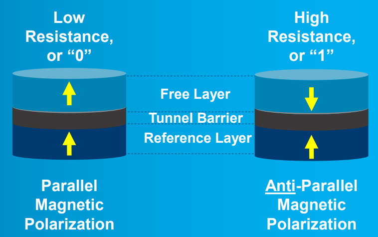
Simplified view of perpendicular magnetic tunnel junction (Image source: Spin Memory)
If we visualize this in its most fundamental form, we have two ferromagnetic plates, each of which can hold a magnetization, separated by a thin insulating layer. One of these plates (the reference layer) is a permanent magnet set to a particular polarity. The magnetization of the other plate (the free layer) can be changed. Each bitcell comprises a magnetic tunnel junction (MJT) and a transistor, and the contents of the cell can be determined by measuring the resistance (low or high) of the cell.
Of course, there are a number of MRAM players in the world, so what makes Spin Memory’s STT-MRAM so “memorable?” (I’m sorry, I couldn’t help myself.) Well, there are a bunch of things, including the fact that the guys and gals at Spin Memory have developed a proprietary precessional spin current (PSC) structure that comprises coupling, spacer, and polarizer layers that are electronically and magnetically coupled to the free layer, where the PSC polarizer magnetization is free to precess.
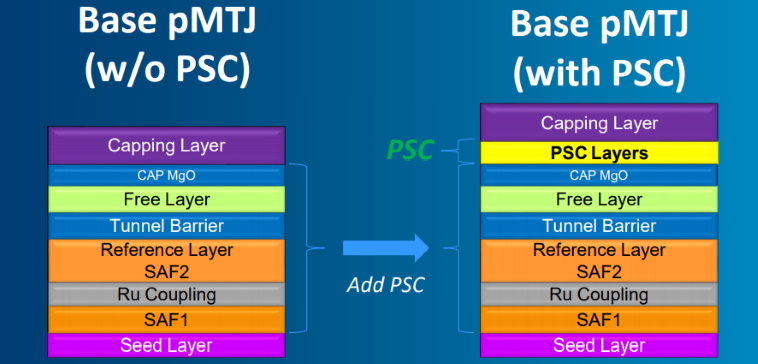
Precessional spin current (PSC) structure (Image source: Spin Memory)
This structure is readily compatible with conventional pMTJ stacks and device processing with no appreciable added cost or complexity, but it enhances the writing and reading processes, and it increases data retention and stability. In fact, while remaining intrinsically radiation tolerant, the folks at Spin Memory say that the use of the PSC structure has been demonstrated to increase the MRAM’s memory retention by three orders of magnitude (1,000 times).
But wait — there’s more, because the clever chaps and chapesses at Spin Memory have also implemented a sophisticated on-chip MRAM controller called the Endurance Engine that performs a host of functions, including detecting and correcting hard and soft errors and boosting performance in the form of increased endurance and increased read/write speeds. By means of “The Engine,” an embedded MRAM (eMRAM) block behaves identically to a block of SRAM in that users no longer have to manage stochastic behavior (e.g., no multiple writes and no need for external verification). The folks at Spin Memory say that “The Engine” has been demonstrated to increase the MRAM’s endurance by five orders of magnitude (100,000 times).
The end result of all this is high density (1/3 to 1/5 the size of equivalent SRAM memory), process scalability (down to the 5 to 7 nm CMOS logic nodes), high-performance (similar to SRAM and faster than DRAM), fully random access (any read/write sequence and any address sequence), zero leakage current, and a memory that is applicable to both emerging and traditional markets (AI, deep learning, neuromorphics, the IoT, etc.).
Spin Memory boasts a world-class team of physicists, scientists, engineers, and technologists. Furthermore, in these troubled times when it’s difficult to know whom you can trust, creators of military, aerospace, and many other applications will be interested to hear that Spin Memory has its own class 100 cleanroom “back-end” prototype manufacturing facility, which is located in Fremont, California, and which features a 100% US citizen process staff.
Personally, I’m tremendously enthused by all of this. I want us (the human race) to get back out into space in person (not just dispatching probes hither and yon), and part of this relies on having sufficient memory to get us where we want to go and letting us do what we want to do when we get there. It may be that, in the not-so-distant future, the systems in our spaceships have labels that proudly proclaim, “Spin Memory Inside!”
If you want to know more about this technology, you can visit Spin Memory’s website, or you may feel free to contact Chuck Bohac, Sr. Director, Business Development (chuck.bohac@spinmemory.com) or Tom Boone Sr. Director, MRAM-Defense and Aerospace (thomas.boone@spinmemory.com). As always, of course, I welcome your comments and questions.


Hi Max! Thanks for the great article. Could you compare Spin Memory’s offering to FMC’s Ferroelectric Memory Jim Turley recently wrote about?
Thanks!
Best Regards, Dave