


The upshot: Accellera has published a whitepaper on the topic of silicon intellectual-property security, and they’re soliciting comments.
Last summer, there were a number of security-related topics at the annual DAC conference, which we covered in August. That activity included Accellera diving into the issue of security surrounding silicon design and, in particular, risks associated with intellectual property (IP) – meaning pre-designed circuits purchased or re-used. It was there that they announced a new working group called the IP Security Assurance (IPSA) group.
A Specific Process
IPSA has made progress since then, publishing a whitepaper on its proposed approach to identifying and mitigating security risks during the silicon design process. This approach modifies the standard high-level design flow and establishes a database referred to as CIPSCE (which I assume to be pronounced “sipsey,” and which stands for “Common IP Security Concerns Enumeration”). We’ll work through the high-level notions here, referring you to the whitepaper for details (link at the end).
Their modification to the design flow is shown below, with the addition of four elements (in yellow):
- Defining “assets” that might be at risk,
- Including references (or “associations”) to the CIPSCE database,
- Defining the vulnerable attack surfaces, and
- Building a threat model.
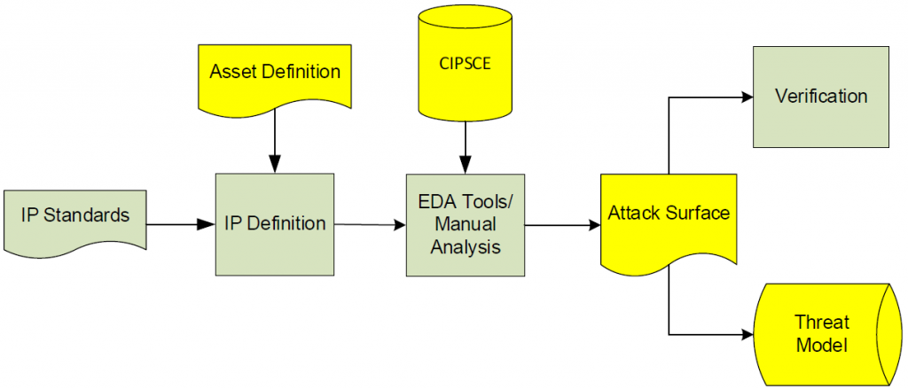
(Image courtesy Accellera)
In this situation, “assets” refer to components within the IP that could be of value. There’s literally a list of 17 families of asset – things like Audio/Video, Microcontroller, and Test/Debug. The attack surface, by contrast, lists the various vulnerabilities that might exist – ways that someone could try to break in. For each asset, one identifies various ways in which someone might try to compromise the asset.
This then works hand-in-hand with the CIPSCE database. Each CIPSCE entry includes a “consequence” characteristic (confidentiality, integrity, or availability), how the threat might be introduced into the design, and how risk from that threat can be mitigated. Each such threat is also mapped to the various asset families to which it applies.
The idea, then, is that well-understood issues and their resolution can be captured in this knowledge base for others to benefit from. It very much resembles other lists of common concerns for cybersecurity. But this also makes it a living list – as new threats are understood, they can be documented there. While useful, this also creates a challenge: between the time analysis on a circuit is done and its use, there’s the possibility of missing threats that might have been identified later. It’s tough to keep designs up to date with respect to all vulnerabilities. IPSA is soliciting feedback and comments regarding how this concern could be resolved.
Roles and Responsibilities
The next high-level question is: who performs all of these tasks, and are they done manualy? It’s important to remember that there are two main design phases that involve IP: the design of the IP itself and the integration of that IP into a larger design.
Much of what’s discussed in the Accellera paper relates to the IP design process. The information assembled can then be of use to someone integrating the IP. Yes, there’s value to establishing this as a discipline for good IP design, resulting in IP that’s more secure. But there’s also value to providing IP users with information on where the vulnerabilities are and how the attack surfaces can be blocked.
One of the take-aways from this summer’s discussion was that, for the time being, the security design process for any design project starts from scratch, with no benefit from prior learning or automation. This new security process might help to address that concern, both by establishing the knowledge base and by providing options for automation. Of course, Accellera as an organization wouldn’t be doing the automating; EDA companies would.
Specifically, they suggest that the CIPSCE associations and identification of attack surfaces could be done by an EDA tool that parses the IP design. Having a robust way of doing this analysis automatically would remove a hugely error-prone manual component of the process. Exactly how that analysis would work, however, is out of the scope of what Accellera would do; this would be up to the EDA companies to find the best techniques.
A number of responsibilities would remain with the IP designer, starting with the initial identification of assets. The proposal includes a table that the designer would fill in – including CIPSCE associations and attack surfaces. If EDA automation of those last two materializes, then the designer could leave those entries blank when doing the manual work, relying on the EDA tool to fill them in.
The designer would then need to package all of this up into the collateral that would accompany the IP for sale (or for re-use). They suggest that this collateral-creation process could also be automated – something that would apply a clean, consistent, and recognizable format for the designers integrating the IP into their larger designs.
That integrator would have a couple of options when acquiring the IP. First, they could use the security documentation as is to decide which of the CIPSCE elements listed applies to the specific system where the IP is used and to test the attack surfaces. Alternatively, they could completely run the EDA tools again to confirm the original list by recreating the CIPSCE associations and attack surfaces as a way of verifying the collateral. They would then also be able to review the latest CIPSCE list to make sure there wasn’t anything that the original analysis missed.
The good news is that this whole process – in whatever final form it eventually takes after feedback and revisions – should add some welcome rigor to what is now pretty much a scattershot process that’s being reinvented daily. The bad news is that, for designers who aren’t worrying about security at all today, this does involve some extra work – even if some automation is available. But, frankly, it’s work that they probably should already be doing, and this will make it easier.
Of course, not all designs are equally at risk. Obviously, designs intended for, say, DARPA will need to be as rock-solid as possible. Other systems, like PC peripherals, might seem to be of less concern. But it’s hard to imagine anything that would be of zero concern. Most components – like peripherals – attach to systems that are connected to other systems, and those innocent, unassuming components might be just the way to break in – not for what’s in the component itself, but for the access it gives to the rest of the system, where more attractive goodies might be found.
The IPSA proposal is open for comment; you can read it in detail at the link below.
More info:


What do you think of the Accellera security working group’s proposal for IP security?