


This has been another “one of those days.” I’ve been discovering all sorts of things pertaining to what’s currently happening in the high-end of artificial intelligence (AI) space (where no one can hear you scream), and now I’m screaming inside and my head hurts.
Let’s start with the concept of an “AI Pod.” This term can mean different things to different people, but it generally refers to a pre-configured, modular infrastructure solution designed to simplify and accelerate the deployment of AI workloads.
These “pods” integrate computing, storage, networking, and software components into a cohesive unit, facilitating efficient AI operations. This is the point where we meet terms like “Scale-Up” and “Scale-Out.” One way to visualize this is as shown below:

Scaling-up and scaling-out (Source: Max Maxfield)
For those unfamiliar with the organization of data centers, a rack is a standardized physical frame or cabinet that holds multiple rack-mounted devices. In addition to servers (e.g., blades), the rack may contain networking equipment (e.g., switches), power management components (e.g., power supplies and power distribution units), storage devices, cooling and environmental control systems, and more.
In the context of this column, each rack may be considered to form an AI Pod. The term “Scale-Up” (a.k.a. “vertical scaling”) refers to adding more resources, such as processors and memory, to a single AI Pod or node. By comparison, the term “Scale-Out” (a.k.a. “horizontal scaling”) refers to adding more AI pods or nodes to the system and connecting them together.
Meanwhile, XPU is a general-purpose term that refers to any type of processing unit (the ‘X’ stands for a wildcard, representing “any” or “all” processors). Example XPUs are:
- CPUs (Central Processing Units)
- GPUs (Graphics Processing Units
- NPUs (Neural Processing Units)
- TPUs (Tensor Processing Units)
- DPUs (Data Processing Units)
- FPGAs (Field-Programmable Gate Arrays)
- ASICs (Application-Specific Integrated Circuits)
For the purposes of these discussions, we will assume that the term “ASIC” embraces System-on-Chip (SoC) devices.
There are typically 2 to 8 XPU devices per XPU blade. Each of these devices may be formed as a monolithic chip (i.e., from a single slice of semiconductor) or as a multi-die system composed of a collection of dice called “chiplets.”
The amount of computational processing power we’re talking about here is mindboggling, as are the XPU devices themselves. For example, NVIDIA’s B200 GPU boasts more than 200 billion transistors (not that I’ve counted them all myself, you understand).
But there’s more to AI than “simply” number crunching data—we also need to move humongous quantities of data around. At a high level, we can think of this as having two primary facets: intra-pod and inter-pod.
Inter-pod communication refers to communication between different AI pods, typically across racks or physical infrastructure units. Intra-pod communication refers to the exchange of information between servers within a single AI pod, typically within the same rack or blade, requiring very low latency and very high bandwidth.
In inter-pod and data center fabric space, the main contenders are InfiniBand and Ultra Ethernet. First released in 2000, InfiniBand was initially developed by a consortium including IBM, Intel, and Mellanox (now part of NVIDIA). Today, InfiniBand is governed by the InfiniBand Trade Association (IBTA). Specifications are published, but NVIDIA and Mellanox primarily drive implementation. By comparison, the Ultra Ethernet Consortium (UEC) was formed in 2023 by a group that includes AMD, Intel, HPE, Broadcom, Cisco, Arista, Microsoft, and Meta, among others. Ultra Ethernet is an open standard aiming for broad industry collaboration and interoperability.
In a crunchy nutshell, InfiniBand has long been the standard for low-latency, high-bandwidth communication, but Ultra Ethernet is rapidly emerging as the open, scalable, Ethernet-compatible alternative for next-generation AI infrastructure.
When it comes to intra-pod communication, NVLink (developed by NVIDIA and first introduced in 2016) has been the historical standard, especially in NVIDIA GPU-based systems, but Ultra Accelerator Link (UALink) is emerging as the future for high-speed, vendor-neutral interconnects across XPUs.
All of which leads us to the purpose of this column (yes, of course there’s a purpose). I was just chatting with Nandan Nayampally, who is the Chief Commercial Officer (CCO) at Baya Systems.
As you may recall from an earlier column (see Weaving State-of-the-Art Chiplet and SoC Fabrics), WeaverPro and WeaveIP are complementary offerings from Baya Systems that are designed to facilitate the design, optimization, and deployment of advanced chiplet-based systems, particularly for AI and high-performance computing (HPC) applications.
WeaverPro (data-driven architecture exploration and optimization) is a software platform that helps system architects design and optimize cache and fabric architectures. WeaverPro supports integration with development environments through SystemC and Python APIs, and its performance analysis capabilities can be applied to actual workloads. It is composed of two main components:
- CacheStudio: Facilitates rapid design and analysis of memory and cache systems, allowing for freeform specification and simulation of workloads to optimize system-level architecture and chiplet partitioning.
- FabricStudio: Enables the design of data-driven, optimal on-die fabric microarchitectures, supporting static and dynamic analysis, and generating physically-aware, correct-by-construction designs.
WeaverIP (scalable, protocol-agnostic fabric IP) is a comprehensive portfolio of Network-on-Chip (NoC) and interconnect IPs that enable efficient, high-bandwidth, and low-latency data movement within and across chiplets. Key features include:
- Multi-Level Cache Coherency: Supports CHI in/CHI out coherent fabrics, facilitating coherent clusters in both single and multi-die systems.
- Flexible Topologies and Protocol Support: Accommodates various network topologies with tiling, Quality of Service (QoS), and protocol clusters, and supports standard protocols such as CHI, ACE5-Lite, AXI5, with extensibility to others, including CXL.
- High Performance: Achieves up to 3GHz operation in 4nm process technologies, enabling petabyte-level throughput in multi-chiplet designs.
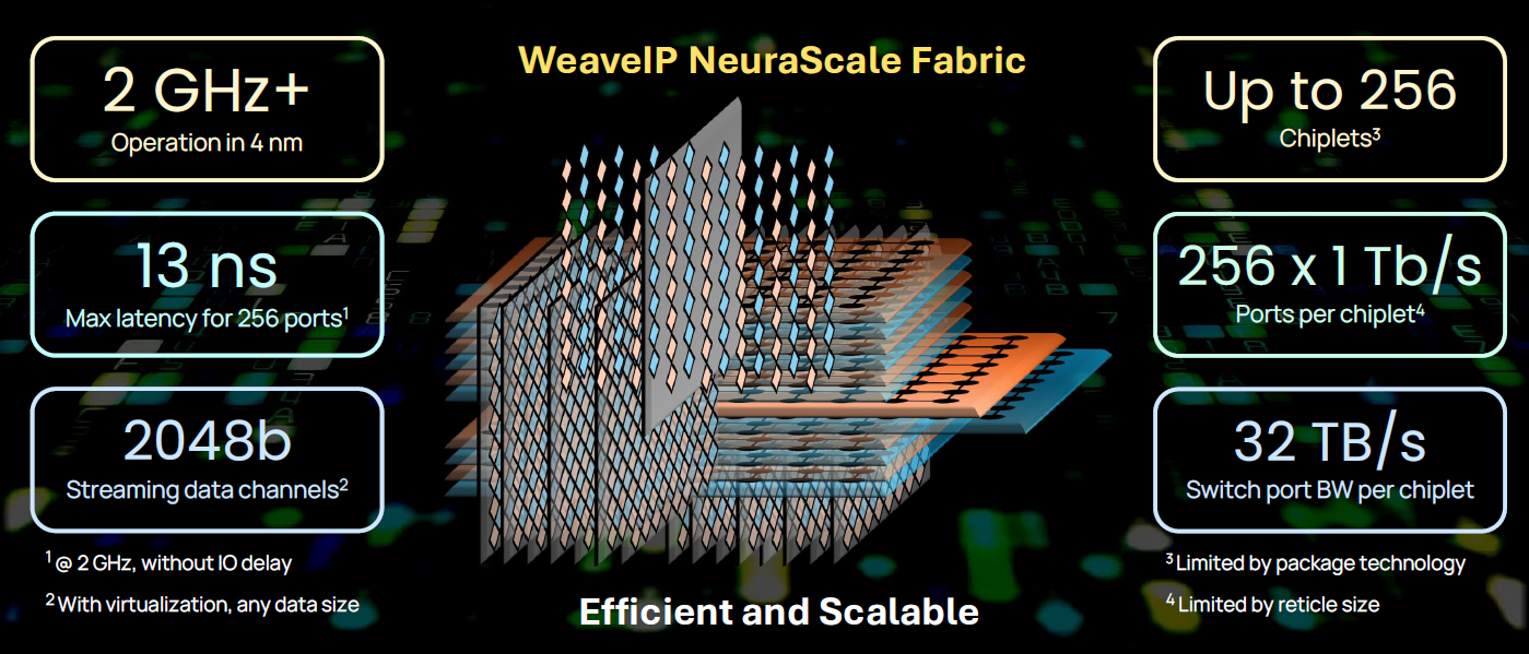
WeaverPro and WeaveIP are already being used to create the XPU ASICs and SoCs (both chips and chiplets) powering the XPU blades shown in the image above, but that’s not what I wanted to talk about. The reason I’m waffling on about all this here is that the folks at Baya Systems recently added NeuraScale scalable switch fabric IP to their WeaverIP portfolio.
Reimagining silicon switching for the AI era (Source: Baya Systems)
NeuraScale, which can be used to create switching fabric on chips (ASICs/SoCs) and chiplets, offers non-blocking, high-port-count connectivity suitable for scale-up and scale-out systems. It’s designed to address critical scaling and data movement challenges in AI infrastructure, particularly for advanced ASICs/SoCs and emerging 3D chiplet-based designs.
NeuraScale technology enables a 100x increase in node density and scale, surpassing present-day systems for next-generation AI with high-density switching. Key features of NeuraScale include support for 256 ports per chiplet with a throughput of 1Tb/s, operation at over 2GHz in 4nm technology, and a maximum latency of less than 20ns. It is also designed to meet future compliance with industry standards, such as UALink, UCIe, and Ultra Ethernet.
O-M-Goodness gracious me, is all I can say. What about you? Are there any thoughts that you’d care to cast into this conversation?


One thought on “Scaling Up and Scaling Out: Reimagining Silicon Switching for the AI Era”