

Over the years (actually, decades, now I come to think about it), I’ve seen a lot of great silicon chip architectures and technologies pop up like hopeful contenders in a semiconductor Whack-A-Mole competition, only to fail because their developers focused on the hardware side of things and largely relegated the software — in the form of design, analysis, and verification tools — to be “something we’ll definitely get around to sorting out later.”
Of course, these companies did eventually cobble some low-level software tools together, something sufficient to allow them to talk to the hardware, but these pseudo-tools could be used only by the designers of the chips themselves because no one else could wrap their brains around how the little rascals (by which I mean the tools, not their creators) performed their magic. Thus, even when these companies had working silicon in their hands, they still didn’t have real-world tools that could be deployed to and employed by their customers. As a result, these companies quickly faded from the collective consciousness like “dust in the wind,” as progressive rock band Kansas sang on their 1977 album Point of Know Return.
I still can’t hear anyone say “Analog FPGA” without a little tear rolling down my cheek. But turn that frown upside down into a smile because I was just introduced to a company called Deep Vision that only recently emerged from stealth mode. Just for giggles and grins, the folks at Deep Vision decided to do things the “wrong” way round — starting by developing a set of robust software tools, including a simulator, proving their architectural concept, and then following up with the real silicon. Having intimate foreknowledge of the software allowed the folks at Deep Vision to ensure that the silicon was created with all the “hooks” required to fully support the software (and vice versa, of course).
One thing I like about the folks at Deep Vision is that they know where they are targeting their technology, which makes my life (with regard to understanding things) a whole lot easier. Consider the power requirements for the various edge AI (artificial intelligence) and ML (machine learning) markets, which might be summarized as follows:
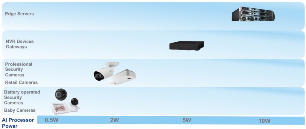
Power requirements for edge AI markets
(Image source: Deep Vision)
As part of their emerging from stealth mode, the folks at Deep Vision have announced their multi-core ARA-1 inference processor, which they say offers the optimal balance of compute, memory, and energy efficiency in the 2W arena.
This is probably a good time to note that, although you and I have only just heard of Deep Vision (and let’s not forget that I heard about it before you, Ha!), they’ve actually been shipping thousands of ARA-1 units to their leading-edge customers for the past six months, which means we aren’t talking about vaporware here.
There are, of course, copious quantities of contenders clamoring for consideration in the 2W amphitheater, so what makes the ARA-1 stand proud in the crowd? Well, I’m glad you asked. The answer is that the ARA-1’s polymorphic dataflow architecture minimizes data movement between cores, within the chip as a whole, and between the chip and the rest of the system. As a result, the ARA-1 offers 4X lower latency than Intel’s Movidius Myriad X vision processing unit (VPU), and 6X lower latency than Google’s Edge Tensor Processing Unit (TPU).
As an aside, the Movidius Myriad X is Intel’s first VPU to feature the Neural Compute Engine, which is a dedicated hardware accelerator for deep neural network inference. Meanwhile, the Edge TPU is Google’s purpose-built ASIC designed to run inference at the edge. The fact that the ARA-1 outperforms both of these devices in terms of latency should make everyone sit up straight in their seats and start paying attention.
When AI is performed in the cloud, it employs predominantly a “throughput architecture,” in which a single AI model performs simultaneous execution on multiple data streams. As its name suggests, this architecture does offer high throughput, but it also exhibits high latency that fails to satisfy real-time inferencing needs. The point is that low latency is of paramount importance for inferencing in real-time, so the ARA-1 provides a “latency architecture” in which “frames” of AI data arrive at fixed intervals, and each AI frame is acted upon by multiple models simultaneously.
What do we mean by multiple models? Well, suppose we have an AI-equipped camera in a department store. Now suppose that we want to track how people move throughout the store and in which products they are interested. Some of the models we might wish to use are person identification, person tracking, pose estimation, product identification, and person re-identification.
Why “person re-identification”? Well, edge scenarios like our store can be very dynamic, with multiple people happily milling around. Suppose we start with a single person ambling around the store, in which case we identify them as “Person A” and observe their movements. Now suppose a second person enters the image and we identify them as “Person B.” If B moves in front of A, then we will have to re-identify A when B eventually moves out of the way (by “re-identify” we mean recognizing that this is the same person we were watching earlier). And, of course, it won’t be long before a herd of additional shoppers join in the fun, meandering around like Olympic milling champions, unwittingly taking it in turns to obscure each other from our view. It’s enough to give you a headache, which is why we wish to hand the problem over to our trusty AI system and then leave it to beaver away while we go and enjoy well-deserved mugs of strong English tea.
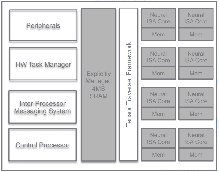
High-level block diagram of the ARA-1
(Image source: Deep Vision)
With regard to the ARA-1’s polymorphic dataflow architecture, this optimizes the data flow layer-by-layer on the silicon, thereby providing tremendous flexibility and control with regard to how applications are implemented. The compiler automatically evaluates multiple dataflow patterns for each layer in the network and selects the highest performance and lowest power option. The Tenser Traversal Engine coordinates work so that resources are fully utilized at all times, thereby ensuring high levels of throughput and power efficiency. Meanwhile, the neural ISA cores boast a novel instruction set architecture (ISA), whereby each instruction executes a micro-dataflow operation, thereby providing maximum data reuse.
As illustrated in the image below, Deep Vision’s software-centric approach facilitates the seamless porting of trained neural network models while also providing deep insights.

Software-centric approach provides seamless ports and deep insights
(Image source: Deep Vision)
The folks at Deep Vision say that the combination of the ARA-1’s polymorphic dataflow architecture with the deep vision compiler results in 10x higher AI compute efficiency as compared to graphics processing units (GPUs). In addition to supporting the seamless porting of trained AI models, the compiler suite provides automated optimization to achieve the best combination of accuracy, performance, and power.
Both silicon and software are built for today’s Edge AI vision applications with the ability to support next-generation AI models, frameworks, and operators. All of today’s industry-standard frameworks are supported, including Caffe, Tensor Flow, MXNET, and PyTorch, along with networks like Deep Lab V3, Resnet-50, Resnet-152, MobileNet-SSD, YOLO V3, Pose Estimation, and UNET.
But wait, there’s more, because we aren’t just talking about a single chip solution – rather a full spectrum of solutions from endpoints to edge servers.

A full spectrum of solutions from endpoints to edge servers
(Image source: Deep Vision)
Now my poor old noggin is buzzing with all sorts of thoughts. Deep learning models are growing in complexity and driving increased compute demand for AI at the Edge. ARA-1 processors are designed to accelerate neural network models’ performance for a wide variety of applications, including smart retail, robotics, industrial automation, smart cities, autonomous vehicles, and more. Keeping data close to the compute engines minimizes data movement, ensuring high inference throughput, low latency, and greater power efficiency. The compiler automatically evaluates multiple data flow patterns for each layer in a neural network and chooses the highest performance and lowest power pattern.
Deep Vision’s software development kit (SDK) and hardware are tightly intertwined to work seamlessly together, ensuring optimal model accuracy with the lowest power consumption. With a built-in quantizer, simulator, and profiler, developers have all the tools needed to support the design and implementation of computationally complex inference applications.
Historically, the process of migrating models to production without extensive code development has been… let’s say… “challenging.” Deep Vision’s solution results in a low code, automated, seamless migration process from training models to the production application, thereby increasing productivity and reducing time to market.
I keep on having to pinch myself and remind myself that artificial intelligence and machine learning were predominantly academic exercises until very recently. In the 2014 edition of the Gartner Hype Cycle — which is used to represent the maturity, adoption, and social application of specific technologies — artificial intelligence and machine learning weren’t even “blips on the horizon.” Just one year later (which is only five years ago as I pen these words), the 2015 Hype Cycle depicted machine learning as having already crested the “Peak of Inflated Expectations.”
We truly do live in exciting times, and companies like Deep Vision are making things more exciting by the day. How about you? Do you have any thoughts you’d care to share about any of this?


