


We’re probably all aware at some level of the new processor upstart, the open-source RISC-V… core? No… architecture? No… instruction set architecture (ISA)? Yeah, that’s pretty much what it is. Which means… if you want to use it, and you’re starting from scratch, then there are lots of steps necessary to do anything.
Given all the hoopla, it’s easy to think that you can simply go out and buy these handy new RISC-V chips, which will cost less, cuz open source, right? But, while excitement is high, an ISA must be turned into an architecture and a micro-architecture, to be followed by detailed chip design and fabrication. And that’s just for the core. Then you need the whole subsystem. At that point, you have a shot at a chip.
Try to use that chip, and you’re going to have to host an OS and then create code and apply middleware and install communications stacks and… and… and… Oh, and then, when you’ve got something working – or, more accurately, partly working – you need to be able to debug the dang thing.
Of course, if you’ve heard of RISC-V, then you’ve probably heard of SiFive, the first really visible company to commercialize RISC-V. But does that mean that this will become yet another single-sourced processor? What if there were options… choices… the kind you get when there is a deep community with real competition?
There are a couple of things buried in that last question: community and competition. NXP has an opinion on the state of the community, and they’re doing some work (for free, at least at present) to build more community. As far as I can tell, their goal isn’t specifically to create more competition, but that could be a side effect of a robust community.
Open-ISA
What they’ve done is to create a new site/community called Open-ISA.org. (Don’t omit the hyphen or you’ll end up on an Ubuntu page!) And they’re hoping to stimulate engagement, both by attracting ecosystem partners and by engaging with designers who are evaluating RISC-V. Their efforts are based on a development board, which in turn is based on a new chip that NXP designed just for this purpose. The chip is called VEGA (making the board the VEGAboard).
NXP is keeping something of a low profile with this – there’s nothing there that they’re specifically selling (although that could change); they’re touting this more as a benevolent thing for the sake of deepening the RISC-V ecosystem. Assuming that’s the case, even though they’ve said nothing specific about any future plans, I wouldn’t be surprised to see something commercial come out of it sometime, if not in the near term. (There’s a limit to how much “charity” companies do… especially when it comes to designing a new chip – not a frugal endeavor!)
In addition to the board, they have a collection of middleware and communication stacks, along with development and debugging tools. Contributing members are:
- Ashling Microsystems, with a C/C++ development platform;
- ETH Zurich, whence the RISC-V cores (more in a second);
- Express Logic, with an RTOS and middleware;
- Foundries.IO, with a complete “microPlatform”;
- IAR Systems, providing another development platform;
- and Seggers Microcontroller Systems, with their collection of development tools, middleware, and debug tools.
And, at present, the board is free. If you’re a developer or an academic (their primary audience), you can simply sign up on the website.
The VEGAries of Computing
The VEGA chip isn’t your typical commercial computing platform; it’s clearly purpose-designed to allow folks to evaluate RISC-V, with another rather well-known company’s cores in there as a baseline. There is a total of four cores: a pair for applications and a pair to handle the communications. Each pair consists of one RISC-V core and one ARM core. For applications, there’s a RISC-V core (more on it in a minute) and an ARM Cortex-M4F (along with a meg of flash, 256K of SRAM, and 48K of ROM). For comms, there’s a different RISC-V core and an ARM Cortex M0+ (with 256K of flash and 128K of ROM).
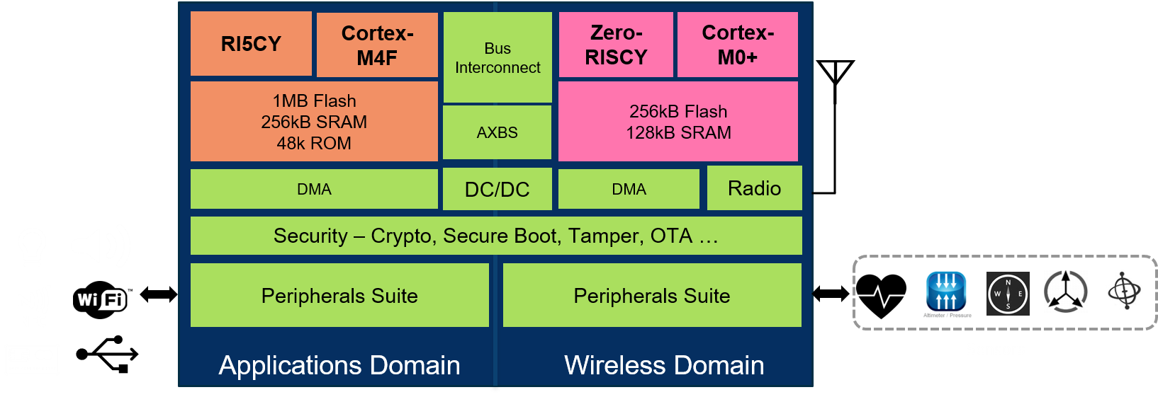
(Image courtesy NXP)
Technically, all four cores can be independently used together, but the cores in each RISC-V/ARM pair share a bus with no arbitration, so that limits everyone running at the same time. Rather than this being a four-core multicore chip, it’s more like a two-core heterogeneous platform, with a choice between RISC-V and ARM for each core. So it would be much more appropriate for comparing apps or comms on one core vs. the other.
Not from Whom You Might Be Thinking
The RISC-V cores themselves aren’t from a commercial supplier, nor did NXP gin up their own cores. The cores they used come from the “Parallel Ultra-Low Power,” or PULP, platform – a project at ETH Zurich. Various different versions exist, and they picked two of them for VEGA. Applications run on the RI5CY core, a 32-bit, 4-stage core. The comms stuff runs on a Zero-RISCY core, 32 bits and 2 stages. The details of the architecture are shown below (you’ll want to click to enlarge it).
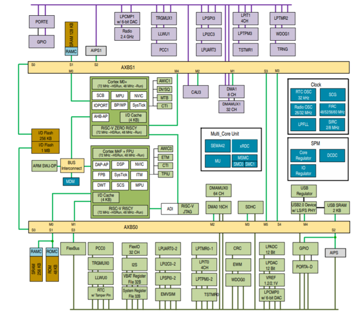 (Click to enlarge; image courtesy NXP)
The board itself provides a connector for Arduino shields as well as a connector for an antenna to support wireless communication. In particular, the radio supports Bluetooth Low Energy 5.0 (up to 8 connections) and IEEE 802.15.4 (giving you ZigBee and Thread at the very least). But they also show support for NFC, WiFi, and other protocols.
The board also supports a range of wired connections, including USB 2.0 and a variety of other interconnects like UART, I2C, and SPI. They’ve layered in security, giving each chip a unique 80-digit ID number and access control to flash. CRCs, cryptography functions, and true random number generation (TRNG) are implemented in low-power hardware.
This has been a quiet announcement by Silicon Valley standards. There was no press release – just a conversation with a few of us newsy folks. Will this catch fire enough to take off? I guess that depends both on whether they’ve hit the right features on the board and whether enough people hear about it. We’ll have to watch and see…
More info:


What do you think of the Open-ISA approach to building RISC-V community?
In short: A RISC is a RISC, ho hum. But this ISA takes the cake for most messy! A true academic curiosity.
I have been looking at the RISC V ISA after having spent 30 years in IBM computer and system development. RISC V instruction decoding is TOUGH, maybe not impossible. And the assembler/assembly programmer really has to do weird things to compensate for no branch less or equal and branch greater than. But nobody programs in assembly anyway.
IBM System/360 had 16 registers, register to register format, and memory/register format that used a much simpler decoding, but of course did not support 64, 128, and 256 byte length instructions. Needless to say RISC V has not figured that out yet either.
It relies heavily on a 12 bit immediate field that only saves loading a value into a register and then using that value in computation. Also branches are relative to the instruction counter plus/minus twice the immediate value. Larger values have to be loaded or constructed first.
There are five different instruction formats because the immediate field is scattered throughout the instruction word. Yet it claims to be load/store architecture. They cannot make up their minds.
There is a separate field to specify the destination register .
There are 2 bits that must be set to one for the base then another 3 bits that must not all be ones because the 64 bit instruction format requires them to be all ones.
But only the 32 bit version is specified and those 3 bits are decoded by the instruction, therefore not clear how to implement 64 bit decoding. And of course the 128 bit format requires another field to be all ones.
ETC, ETC, ETC.
I’m not sure what you are looking at, but it doesn’t seem to be the RISC-V I know!
The instruction decoding is *very* simple. Amateurs have been implementing RISC-V processors in FPGAs using as few as 306 LUT4s.
The fields for the destination, source1, and source2 registers are in the same place in every instruction format (or which there are basically four) in which they exist — on almost every other CPU the destination of a load and the source of a store are encoded in the same place, complicating decoding. The MSB of literals is always in bit 31, so it’s easy to get started sign-extending it early. There are 12 bit and 20 bit literals/offsets and they are treated a little differently depending on whether they are for arithmetic (the obvious straightforward encoding) or a branch offset (yes, it looks a little scrambled) but the net effect is that in the final 32 bit value there is one (1) bit that can come from three different places in the instruction, and all the rest can come from at most two different places in the instruction, or from a constant 0 or sign-extended source.
“And the assembler/assembly programmer really has to do weird things to compensate for no branch less or equal and branch greater than”
It’s true there is no BLE or BGT binary instruction, but if the programmer writes “BLE rA, rB, target” then the assembler simply outputs the instruction “BGE rB, rA, target” instead. There is no need for the programmer (or even GCC) to hurt their brain with this.
Similarly the assembler provides a number of pseudo opcodes including j, jr, ret, nop, mov, not, neg, sext.w, beqz, bnez, bltz, blez, bgtz, bgez, snez, seqz, sltz, sgtz, fmv, fabs, fneg that don’t exist in the instruction set but can be implemented with a single instruction with typically a zero immediate/offset and/or the Zero register.
The complaint about the instruction length encoding is a bit baffling. It’s *directly* inspired by the two bits in the IBM 360 encoding that specify 16, 32, or 48 bit instructions. It’s just rejigged a little to give three times more 16 bit instructions (48k) than the 360 has of RR instructions (16k), and the possibility to have instructions longer than 48 bits. No one has implemented a RISC-V processor with anything other than 16 and 32 bit instruction so far, in which case it’s very easy: if the 2 LSBs are ’11’ then it’s a 32 bit instruction, otherwise it’s a 16 bit instruction.
“It relies heavily on a 12 bit immediate field that only saves loading a value into a register and then using that value in computation. Also branches are relative to the instruction counter plus/minus twice the immediate value. Larger values have to be loaded or constructed first.”
This is perfectly true, but misses the fact that it only takes one extra instruction to load, store, or branch to any absolute or PC-relative address in a 4 GB range.
“There are five different instruction formats because the immediate field is scattered throughout the instruction word. Yet it claims to be load/store architecture. They cannot make up their minds.”
This is a complete non sequitur. A load/store architecture is one in which arithmetic is done only on registers (and immediates), and loads and stores do not do arithmetic. It has nothing to do with the instruction encoding.
To be clear, there are four instruction formats because different instructions need:
– a destination register and two source registers (arithmetic)
– a destination register, one source register, and a 12 bit literal. (loads, arithmetic with an immediate, and indirect function calls/branches)
– two source registers, no destination, and a 12 bit literal. (stores and conditional branches)
– a destination register and a 20 bit literal. (unconditional relative branches and loading the upper part of absolute or PC-relative constants/addresses)
That is all that is logically necessary, but branches (except indirect) multiply the 12 or 20 bit literal by 2 to increase the branch reach.
As previously mentioned, the destination and the two source registers are always in the same place in the instruction, if they are present. The encoding is designed so that when rs2 and/or rs1 are not present in an instruction format the literal/offset takes over that field and forms a larger contiguous group of bits. However in the format with no destination register (stores and conditional branches) the literal/offset necessarily is split into two non-contiguous parts.
Most programmers of course need not pay any attention to this, just as they don’t on other ISAs. No one reads instructions in binary, you use a disassembler.
I disagree:
“This is a complete non sequitur. A load/store architecture is one in which arithmetic is done only on registers (and immediates), and loads and stores do not do arithmetic. It has nothing to do with the instruction encoding.”
Where is the official definition of load/store architecture? Are you absolutely sure that intermediates are included? Were they just added because …. (they were not specifically excluded)?
“To be clear, there are four instruction formats because different instructions need:
– a destination register and two source registers (arithmetic)”
Accumulator and stack machines do not need 3 architecturally visible registers. Does this mean they cannot do arithmetic? (one register can be a source as well as the destination) i.e. accumulator or Top of Stack.
Also the code points for BLE or BGT are available, just not used. Because the assembler takes care of it … as if anybody actually codes in Assembly. Today’s world is full of programming languages that are being used.
Scala is being used for RISC V hardware design for similar reasons, I think. Probably because System Verilog is a dog, or maybe Scala is a Berkeley creation?
I am looking at this thing primarily as a computer designer. And it is easy to understand why no one is designing a 48 or 64 bit version.
Then there is the compressed format that the assembler tries to turn into a 32 bit except that 16 registers are missing………
I also beg to differ!
@Brucehoult already confuted many of your points, most of which you ignored.
The ones you retorted are weak points I think.
– You replied to Bruve that there is no official definition of a load-store architecture, the term itself is hazy. Then, maybe, don’t imply in the first place it is not a “true load-store”, because it’s quite self-contradictory.
– Compressed format with 16 registers? – (C)ompressed format extension, and the (E)mbedded version (with 16 instead of 32 regs) are separate options. Although it makes sense to choose both one in embedded applications. Still, what is the problem with that?
You did mention that IBM 360 had 16 regs – did you mean it as a pro over RISC-V, because it sounded like that? So, is it good to have 16 registers, or not? Who said something about “making up their minds”? ARM’s embedded cores have 12 (not really) general regs, so the RISC E is a 33% more generous than the now industry standard, I certainly see no problem with that.
– Tough, maybe not impossible to decode? Good thing we have geniuses all over.
Let me try to phrase this again. NXP/Freescale did make RV32M1 (Vegaboard), because it is such a tedious and gate/power consuming ISA, that devs should compare this: two RISC cores (low and even lower level) with two ARM cores (Cortex-M4F and a Cortex-M0) packed into the same chip, with access to the (pairwise) same peripherals. Yeah, they’ve built (and selling!) the best comparison possible, because it is SO bad. Sorry, but I’ll think I’ll believe the resulting benchmarks instead of your opinion.
The instruction formats clearly have a not too good-looking optimization, I agree.
But most optimization is a trade-off and I don’t know about this one enough to have a strong opinion.
Neither do I know about that BLE and BGT is better left out, or not.
But arithmetic without dedicated destination register is almost 100% a bad design now – it’s shelf life has long expired. Back to ARM- no surprise they have Rd too.
Overall, this ISA seems to be much saner to me, than the ARM embedded ones – that’s what I know the most, and even though it has its own big drawbacks, I though it was the best at hand.
I won’t be super sad if NXP releases some Cortex-M alternative chips with RISC-V and their analogue stuff, which will prove themselves better than what I loved to use.
Others archs have their own batshoot-crazy things, not not mention that from the three most currently popular ISA, two (ARMv7 and x86) are not even classically virtualizable, which is quite the turn-off nowdays.