


Their first job was to soften up the target. They did that using paratroopers who prepared the scene quietly and unobtrusively. Once that was done, the bombing campaign could begin in earnest.
In the era of fine feature resolution, sometimes it’s necessary to refine our processing tools. After all, backhoes are good at digging holes, but they’re not OK if you’ve shrunk the size of the hole to a couple of inches across; you need something more precise.
Rather than a backhoe, we have three silicon processing categories: adding material, patterning, and removing material. We’ve talked patterning to death, what with the drama surrounding extreme-UV lithography. As to adding material, the gentle approach these days is to work atomic-layer-by-atomic-layer, using – duh – atomic-layer deposition, or ALD. But what about removing material?
It stands to reason by natural symmetry (even if it’s scientifically unreasonable reasoning) that we should also remove materials one atomic layer at a time. Sounds good, but is it physically possible? Why, yes it is. It’s called – surprise! – atomic-layer etching, or ALE.
In a series of conversations with Lam Research, I got a picture of how ALE works. It’s actually quite intuitive as a concept, although, clearly, the details and the math matter. I’ll leave those latter bits to Lam, but we don’t really need them to get a feel for what’s going on.
Incumbent Etch
Let’s start with what the default etch methodology is. We’re going to focus on plasma (or dry) etch, which has been a tool for directional (anisotropic) etch since the 70s. So-called wet etch also still has a role, but that’s more often used for isotropic etch – not what we’re going to look at today.
Roughly stated, the idea with plasma etch is that you take gaseous reagents and turn them into a plasma, thereby cranking up the energy so that you can etch quickly enough for commercially viable throughput. A number of things happen to those reagents in this environment, with two being particularly important:
- Some of them form radicals that can chemically combine with whatever it is you’re trying to etch.
- Some of them form ions that physically bombard the surface to remove material.
It turns out that there are tons of different “species” created in this process. We understand the main ones and how they work, but there are probably a bunch that we can’t track in detail. It all just sort of works. (It brings to mind Maillard reactions, where you get hundreds of compounds as you cook…)
The thing is, though, that this stuff all happens together at the same time. You’ve got surface reactions going while stuff is being removed and other possible minority side reactions going on, all of which make something of a sludgy layer at the etching interface. When removing large quantities of material, it hasn’t historically mattered. But for super-precise dimensioning, it’s less than ideal when fine-tuning something like a delicate FinFET gate. It’s just a bit too chaotic for that.
Taming the Chaos
Let’s say we want to etch an atomic layer of silicon. We have a couple of options.
- The easiest one is to wait for the silicon to etch itself. Yeah, in theory, silicon atoms could sublimate away. But… ain’t nobody got time for that. So… ‘nuf said about that.
- We could just blast it with something to physically eject (aka sputter) silicon atoms. A couple of issues here: that takes a lot of energy, and you can’t do only one layer; you don’t have fine control.
We need something subtler, and neither of those options qualifies as subtle. What we can do instead is to break the etch-all-at-once process into two sequential steps. Yes, it very much resembles ALD in this and other ways.
The first step involves reacting our material – silicon in our example – with something else so that the resulting molecule is easier to remove than the silicon is by itself. Chlorine is a common way of doing this with silicon, and it makes SiCl2.
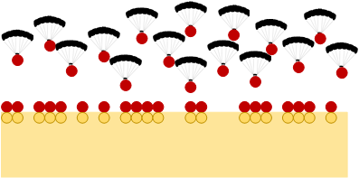
Parachuting in a reagent to modify the surface
The second step involves simply bombarding the surface with ions (no reagent) to dislodge the modified molecules.
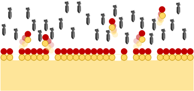
Bombing the surface with ions to remove the modified material
Do these two steps, in order, over and over, and, at some point, you’ve removed all the modified material, and you stop. The mental construct is that each of these cycles removes one atomic layer.
In practice, though, it’s not usually quite that simple. Take silicon, for example. When the chlorine reacts, it first forms SiCl; that stops once the surface is saturated. Then one silicon will steal a chlorine from a neighbor to make SiCl2. So now you have an unreacted silicon atom where a SiCl used to be. The second step removes only the SiCl2, meaning only half of the silicon atoms on the surface (those bound with two chlorines), and so you’re removing a half-layer. But that’s a technicality; the mental construct is still useful.
Don’t Go Too Far!
What’s compelling about this – no, more than compelling: essential – is that each of these steps is, in theory, self-limiting. The first step reacts only with the top surface layer; once that’s covered, the reagent (like chlorine) can’t get to the atoms underneath the surface, buried in the crystal (not to mention the fact that the inner silicon atoms don’t have free bonds the way the surface ones do). So the first step stops when the surface saturates.
The second step is intended to remove only the modified molecules, not the raw silicon. So, once all of those molecules have disappeared, then, in theory, you can keep bombarding away and nothing else will be removed.
This all works, however, only if energy levels are right. The idea of the first step is to create an intermediate product that is removed with less energy than silicon would be by itself. But you want to create that product in a controlled way that doesn’t also remove the SiCl2 after it’s formed– that’s reserved for the second step. So you need enough energy for the reaction, but not so much as to dislodge things.
In the second step, you can give it more oomph and eject the intermediate product. But if you blast away at it too hard, then, even after you’ve removed all of the SiCl2, you may also end up sputtering away pure silicon. If that happens, you’re no longer self-limiting, and you no longer have the precision you want.
These energy relationships must be in place for this to work. This helps to determine which materials you can etch like this, as well as which reagents and intermediate products can be used.
Yet Another Cyclical Process
ALE thus joins other cyclical processes like ALD and deep reactive ion etching (DRIE). If you’re really impatient, you might get tired of waiting for the back-and-forth and be tempted to come in there with a chisel to get rid of stuff real quick-like. But in those applications where you need to be very precise, it’s fast enough to be commercially viable. Heck, it might get faster over time as we refine how we do it, but, even as it is, it’s being used now in production on leading-edge nodes.
More info:
Atomic Layer Etching: Rethinking the Art of Etch, the Journal of Physical Chemistry Letters


Do you use ALE? Which steps do you use it for?