


Another day, another patent lawsuit. It’s just one of the many tools in the Silicon Valley (and any other global Silicon Situ) toolbox. So an announcement by Nikon that it is suing ASML and Zeiss shouldn’t raise too many eyebrows, right?
Well, yeah, except that, in this case, Nikon might as well be saying that they have a patent on sand. And… as with all things legal, I should probably clarify my meaning there. I’m not saying that it’s a “worthless” patent (or set of patents), but rather that it’s fundamental to anything semiconductor today. Like sand is.
Specifically, Nikon is saying that immersion lithography is their baby and that ASML has made hay with it. And, to clarify my meaning, this isn’t to say that I suggest using babies to make hay. They’re just expressions, and if you insist, yes, they constitute a mixed metaphor. Thanks for asking.
For those of you fortunate enough to have someone else build your chips without you having to worry about how it’s done, let’s review briefly what the deal is with immersion lithography. (No, it’s not high-tech waterboarding.) For those who already know this stuff, feel free to skip to the next section (thereby missing any goofs in what follows).
Technology That’s All Wet
Lithography means using a mask to break up a light beam so that you, in effect, take a picture of a circuit layer and print it onto silicon that’s been coated with light-sensitive goop. Now, if you’ve ever taken a picture of, say, Mt. Rushmore, but, in your youthful exuberance, went wide angle to capture the faces in the context of the grandeur that is the Black Hills, and then looked at the print later and grumbled that the faces were tiny and you couldn’t make out the details, then you know that small features don’t always print.
Posterity might forgive a poor image of Mt. Rushmore, but a poor print on silicon is a problem. As features get smaller, we need to expose the wafers with shorter-wavelength light. That’s been the whole deal with extreme ultraviolet (EUV) litho: incumbent technology uses light with a 193-nm wavelength; EUV is going with 13.5 nm. (For reference, visible light runs out of steam at 400 nm, so today we’re already in the UV realm – merely “deep” (DUV) rather than “extreme.”)
This is governed by a simple equation for minimum resolution R:
![]()
Clearly, the smaller the impinging wavelength λ, the smaller R will be. But let’s just say that EUV has had somewhat of a longer gestation than anyone expected. So, for the moment, we’re stuck at 193 nm. That equation might suggest that miniaturization would come to a halt, except for that denominator thing: the numerical aperture (NA). This is a property of the medium through which the light travels as completes its last leg onto the wafer. If you can make that bigger, then it provides another knob for reducing R.
The NA has to do with the widest angle from which light can be collected (in the case of a microscope) or dispersed (in our case). In the image below, you can see that any light going from the first medium on the left to the second at an angle greater than θ1 will miss the second lens, so that makes it look like a function of the setup. But even if you have an infinite second lens, there’s still a limit: if you go too wide, you end up with photons skipping off the surface of that first element (n2) like so many smooth, flat rocks hopping across a river.
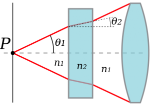
(Image source: Wikipedia)
Normally, that last distance the light travels is simply the air between the light source and the wafer. But replacing that air with liquid, you end up with a different NA – and a larger one. That’s the whole idea of “immersion”: the light path is immersed in liquid up until it hits the wafer. That liquid could be a lot of different things; at present, it’s purified water. So even with 193-nm light, you can now resolve smaller features than was possible before.
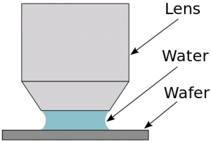
(Image source: Wikipedia)
This technology is typically shorthanded as 193i. And. It’s. Everywhere. If you’re on a 45-nm process node or beyond, you’re using 193i. It’s as fundamental to leading-edge chips as sand is. It might look simple, but there are lots of details surrounding how you manage the liquid and temperature and wafer positioning, and those are the patents in dispute.
Legal Flurries
Nikon would appear to be the inventor of this whole shebang. Just to clarify my meaning, I don’t know that they’re the inventor; I have no independent proof that they’re the inventors; and I’m not trying to prejudice any would-be jurors – but I have seen granted patents, and I haven’t seen (yet, anyway) anyone disputing this technology genesis. So I’m moving forward with that as a provisional assumption.
All good so far. Except that, somehow, while no one was looking, ASML came in and, eventually, dominated the business.
Actually, someone did notice. Nikon sued ASML in 2001; they settled out in 2004. According to Nikon, old patents were cross-licensed in perpetuity; more recent patents were licensed to expire at the end of 2009. And they decided on a temporal demilitarized zone: a period of time when they both promised not to sue each other – even if they thought it might be merited – from the beginning of 2010 through 2014.
And, meanwhile, the patents and equipment kept coming – including during the no-sue times.
So, the exclusion period ends, and what happens? There are two very different views of the negotiations that then occurred. According to Nikon, “… Nikon has attempted to negotiate with ASML and Zeiss to reach agreement on a new license agreement. However, ASML and Zeiss have not been willing to accept terms reflecting the value of Nikon’s patented technology.” According to ASML’s initial response, “ASML has made repeated efforts to negotiate an extension of its patent crosslicense agreement with Nikon[.] Nikon has not engaged seriously with ASML and has instead chosen to commence legal proceedings”
I tried to reconcile those views by checking in with both ASML and Nikon. ASML provided the following specifics:
- “During 2009, before the expiration of the cross-license, ASML proposed that executives from each company meet to discuss the terms of a renewed cross-license. Nikon refused, contending that ASML’s request to negotiate a renewed cross-license was premature.
- “ASML renewed its request near the end of 2013, and into 2014, again proposing that executives from each company meet to discuss the terms of a renewed cross-license. Nikon again refused such a meeting.
- “In 2015 and again in early 2016, ASML proposed mediation. Nikon refused to engage meaningfully in the mediation process.”
I contacted the company handling Nikon’s communications to see if they agreed with this picture of events. They were going to respond, but I haven’t received a response as of my deadline. If I receive one later, I’ll update.
Markets vs. ROI
OK, so that’s how this current brouhaha spun up. But it’s emblematic of one of the major challenges of this kind of technology: there’s no real market in the way we expect for retail goods (although those look less and less like real markets too, what with all the consolidation).
Thirty years ago, there was this notion of “second sourcing.” Many purchasers of electronic components would not consider using something new and innovative if it was available from only one company. Too risky; if that company went belly-up, they’d be stuck without a way to get components, and they’d have to redesign.
Oddly enough, then, a company with innovative ideas would actually encourage some other company to compete. If they did it shrewdly enough, they’d pick a competitor that was just credible enough, but one that would hopefully not do too well. They could then check the “second source” box, make the purchasing guy happy, and, in theory, still dominate sales.
Well, that’s a quaint notion today. I came from the programmable logic field, and we went from small stuff with second sources to the two major monoliths – Xilinx and Altera (now Intel) – which were decidedly not pin- or anything-else-compatible. The entire industry transitioned into a world where you weren’t buying chips in a commodity market (“commodity” being a dirty word), but rather you were partnering with specific companies and technologies, hoping that you’d bet on the right horses.
And the farther along we’ve come, the more complex and expensive development has become.
To the point where we’ve really lost much of the notion of competition. Yes, companies still compete, but not in an ongoing market with ebbs and flows. It’s a winner-take-all battle, and the only question is which company will ultimately dominate.
Some areas, like cell phones, are competitive from the OEM standpoint, but not from a technology standpoint, it’s Apple and Google (Android). Search engines? Yeah, Google. Retail? Amazon wants all the sales. Period. Ride-hailing? We exalt Uber, despite its poor behavior (which apparently has taken some cues from VW’s playbook). Yes, Lyft and others exist, but they struggle to be heard above the One Big Guy.
Investors love this “one winner” scenario – as long as they picked the winner. When pitching to VCs, it’s important to know who the current Big Winner is. If everyone is talking about the amazing new things McWidget is doing, then you start your pitch with, “We will be the McWidget of [state your business here],” and all of the investors that missed out on the first McWidget opportunity will be aching to correct that situation, improving your chances of getting funding.
And that’s in the consumer space. Within the engineering space, it can be similar with fundamental enabling technology. (Yeah, the grommets and washers used on fancy equipment are probably still commodities – at least until they come up with internet-connected ones…)
I’ve often wondered whether the EDA space would approach a singularity. Each generation of technology becomes more expensive to develop – and, these days, to manufacture. Which means that fewer companies can afford to buy it. Which makes the market smaller (in terms of participants). Taken to its limit, you have infinitely expensive software that no one can afford. Like a technological black hole, all the money goes in and none comes back out.
Of course, so far, there’s no event horizon in sight. We still have three big companies competing with each other. But, then again, to think that three companies makes a rich market says something about the state of “free” markets these days.
So here we have Nikon, which developed a critical methodology for continued miniaturization while EUV was getting sorted. And let’s be clear about this: developing new technology is expensive, and no one would do it if they thought they’d never see a return on that hefty investment. In fact, that’s the essence of the problem: the further along we go, the more expensive things are. That means fewer companies being able to do their own R&D. And it gives those companies that can invest more reason to protect that investment with patents and lawyers.
This is a variant on what happens with technology standards. These days, if a standard depends on some critical enabling patented technology, then the patent owner needs to make licenses available on a “reasonable and non-discriminatory” (RAND) basis. That means you can’t charge the company you don’t like ten times what you charge the company you’re not threatened by. Absent this agreement, the standard won’t proceed.
Things weren’t always this way; there were some notorious cases of “submarine patents” that weren’t disclosed during the standardization process, and, after the standards were set, then the patent owners could make hay with licenses. (No babies.)
So, if a standard is involved, it’s likely that critical technology will be available for use. But there is no official lithography standard; there’s simply the way we do things. Roadmaps are created and debated by the industry as a whole, as exemplified by the International Technology Roadmap for Semiconductors (ITRS). This happens years before anything is built, and it’s tweaked on a regular basis as erstwhile projections become reality. It gives everyone an agreed-upon target to shoot at. But, critically, it’s not a standard. There’s no expectation of RAND.
Look at EUV: it’s astounding the total investment that must have gone into this. When I started paying attention a few years back, there were a few companies with competing ideas for sources of the EUV light. Ultimately, it became an all-Cymer discussion – which was further solidified by ASML buying Cymer. You don’t hear much about most of the alternatives at this point, although Gigaphoton gets occasional mentions as a second source.
But there’s so much new technology in an EUV light source that there’s practically no way for some other company to catch up and still avoid all the Cymer/ASML patents. The industry has pretty much crowned ASML as the sole provider of EUV technology – because we’re so hungry for eggs that we’re ready to put them all in the one basket that doesn’t seem to have holes in it.
Of course, patents run out. At some point, existing Nikon and ASML patents will expire. Someone else can then jump in. But things are moving so quickly that, by the time a patent expires, it will likely have been replaced by a new patent that keeps things relevant. There may be scraps available based on the old expired patents, but it’s not like there’s a generic market in the way there is with drugs. 20 years from now, we’ll be slaying different dragons; expired patents will have nominal value.
So that’s why this lawsuit caught my eye. If Nikon were able to stop ASML making 193i equipment, it would constitute a severe disruption. Which everyone knows, of course. So the lawyers will push it to the brink… and then settle on something. Or that’s my guess, anyway.
Another day, another patent settlement. It’s just one of the many tools in the Silicon Valley toolbox.
Coda: Right before this went to “print,” ASML’s informal response of a few days ago was followed up by a formal announcement of their own countersuit. A few minutes later, Zeiss announced their countersuit. It’s officially a party.


What do you think about the 193i patent situation, or the broader technology implications?