

“Time moves in one direction, memory in another.” – William Gibson
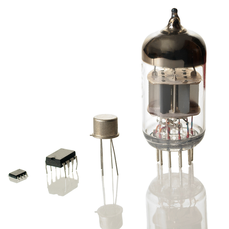
Memory is different from logic. We learn this early in our careers, especially if the job involves fabricating one or the other. Logic gates scale. Memory cells scale, too, but not the same way. In extreme cases, we even do multi-chip modules or flip chips just to keep the memory and the logic apart. Intel makes logic ICs. SK Hynix makes memory chips. Different fab processes. Different recipes. Never the twain shall meet.
Unless…
What if I told you that logic and memory were the same thing? And not just in the sense that a flip-flop is a one-bit “memory” for as long as the power stays on. I mean a nonvolatile memory that’s built on a logic process, right alongside the rest of the logic. Out of transistors, not specialized memory cells. A nonvolatile CMOS transistor.
That’s the promise of Ferroelectric Memory Company, a German startup that has developed a nonvolatile memory technology that’s fabricated just like logic transistors, but with a special ingredient. (Hint: it’s right there in the name.)
The company is a spinoff from the Technical University of Dresden, which acquired some of the assets of the now-defunct Qimonda, which used to be part of Infineon, which used to be part of Siemens. So, long history there. During its short life, Qimonda made DRAMs and flash memory, but strangely, the nonvolatile technology grew out of the DRAMs, not the flash. The company developed an oxide for its high-k metal gate (HKMG) process that becomes ferroelectric under certain conditions. The company filed two fundamental patents on the discovery but never commercialized it.
That job fell to the Ferroelectric Memory Company (FMC), which was founded in 2016 after licensing the Qimonda patents and raising money from European investors. The secret ingredient is hafnium-oxide (HfO2), which is already common in both logic and memory processes. What’s new is the discovery that the material has “a previously unexpected crystal phase” that holds its oxygen atoms in one of two stable states. Furthermore, it’s easy to coax those atoms into either state by applying a small voltage. Because HfO2 is already used in semiconductor fabrication, it doesn’t contaminate the process or add dozens of bizarre new steps.
Best of all, you don’t have to fabricate dedicated memory cells with it. You can build normal transistors that just happen to double as nonvolatile memory cells. FMC calls these FeFETs, for ferroelectric field-effect transistors. If you made nonvolatile FinFETs, you’d have to call them FeFinFETs.
FMC says its FeFETs scale right along with normal logic transistors, so there’s no penalty for mixing your memory and your logic on the same die. You can also place FeFETs directly next to logic gates – there’s no keep-out area or boundary required – which opens up some interesting possibilities for memory placement. If the NVM doesn’t have to be segregated in large blocks, you’re free to mix it indiscriminately with your logic.
Initial indications are that FeFETs are faster than conventional flash memories, at about 25ns for both read and write. And they use less power. A FeFET transistor is switched by applying voltage, not current, so it uses less energy than a NAND flash, and there’s no such thing as an erase cycle.
The company’s plan is to license its technology to foundries, not to sell standalone memory chips. It’s conducting trials with two foundries so far, GlobalFoundries and “a famous Asian foundry” that it declines to name. GloFo should be ready to offer FeFETs to its customers in about two years, FMC figures. That places products in consumers’ hands in 3–4 years. That should be enough time to erase several flash drives.


