


Ever since I began my career in electronics, analog has been the underdog compared to digital in the realm of automation. In the case of tools and techniques like fault simulation, test coverage, and automatic test pattern generation, the digital world has enjoyed robust support for decades. Meanwhile, analog has typically been relegated to handcrafted efforts and ad-hoc methods. Well, that imbalance just shifted in a dramatic fashion.
Analog and digital designers and verification engineers talk different languages and are invited to different parties. This column is unusual in that it should interest almost everyone involved in the design and test of ASICs, ASSPs, and SoCs that contain any amount of analog functionality (and don’t they all, these days?).
Since many analog guys and gals are unfamiliar with what’s possible with things like fault simulation and automatic test pattern generation (because they’ve never seen anything like this in the analog world), let’s start by briefly describing the evolution of tools and techniques used in the digital domain, and then we will discuss how the analog world just caught up in a big way.
From the 1970s through the early 1980s, fault simulation was one of the earlier systematic approaches to testing ICs. My own involvement with this was with the HiLo simulation suite. This originated in the UK at Brunel University in the late 1970s and was later commercialized by Cirrus Computers (which was eventually acquired by the American company GenRad).
HiLo itself was a digital logic simulator. This was accompanied by the HiTime timing simulator and the HiFault fault simulator.
To utilize any of these simulation engines, we began by capturing a gate-level netlist (later augmented to support the register transfer level (RTL) of abstraction) and creating a set of test vectors. These vectors specified the signals to be applied to the inputs and the corresponding signals expected at the outputs. In the case of HiTime, the simulator automatically applied stuck-at, open, and drive faults to the gates and wires forming the circuit.
Stuck-at faults occur on wires and represent a short circuit to a ground plane or power supply. Drive faults occur on gate outputs, which are driving logic 0, 1, or Z (tristate) values. Open faults occur on gate input terminals, which may “float” to 0, 1, or Z.
On the off chance you’re interested (and the even “offer” chance you can lay your hands on a copy), I discussed all this in excruciating exhilarating detail in my book Designus Maximus Unleashed (Banned in Alabama).
But we digress. When you ran HiFault, it applied the aforementioned faults to the gates and wires forming the netlist and ran your test waveform to see whether those faults propagated to the chip’s outputs. As part of this, it provided a coverage report detailing which portions of the design were tested and which parts remained untested. This was an iterative process in which we reviewed the results and adjusted the test waveform accordingly.
Once you have fault simulation, which initially required creating test vectors by hand, the next logical step is automatic test pattern generation (ATPG), which also emerged during the late 1970s and early 1980s. ATPG worked in conjunction with the fault simulator. Now, instead of just simulating faults, ATPG could be used to generate specific vectors to excite and observe each modeled fault.
By the mid-1980s, dense IC packaging made probing pins on a PCB nearly impossible. This led to the formation of an industry consortium known as the Joint Test Action Group (JTAG) in 1985. In turn, this led to the introduction of boundary scan. The idea here was to add a shift register cell to every input and output on every (significant) IC. This allowed the states of the chip’s pins to be set and read via a serial interface. The access mechanism was a 4-pin test access port (TAP). In 1990, the IEEE standardized boundary scan, and the entire package, including the TAP and boundary scan cells, became known as JTAG. Over time, people began to use “JTAG” less to refer to the boundary scan standard and more to refer to the TAP interface.
Boundary scan was focused on board-level tests. When it came to testing the devices themselves, ATPG needed controllability and observability of internal flip-flops. The solution was to convert any flip-flops inside the chip into “scan cells” and connect them together to form “scan chains.” In the case of a “partial scan,” not all flip-flops are scanned (due to area/timing overhead), but this still makes ATPG practical. In the late 1980s and early 1990s, it became practical to implement “full scan,” in which every internal flip-flop is made scannable. During testing, the chip appears to be one or more giant shift registers, making ATPG significantly easier and offering much higher coverage. This became the mainstream design for test (DFT) methodology for digital ICs in the 1990s, and it is still the workhorse today (enhanced with sophisticated compression and other techniques). Meanwhile, the JTAG TAP was reused as a convenient port to access the on-chip scan chains for ATPG and to control features such as built-in self-test (BIST).
As we see, design, test, and verification were very exciting in the 1970s, 1980s, and 1990s. At least they were for digital designers like your humble narrator (I take pride in my humility). Meanwhile, in analog space (where no one can hear you scream)… nothing much happened. Well, the SPICE analog simulator “happened” in 1973, but that was about it as far as I was concerned (I can visualize analog engineers gnashing their teeth and rending their garb when they read this, but that’s all right because they don’t know where I live).
One more thing we need to discuss before moving on to the meat of this column is the difference between “structural test” and “functional test.”
In digital circuits, structural test means verifying the integrity of the hardware’s structure using scan chains, ATPG patterns, and fault models such as stuck-at faults. The goal is to systematically detect potential manufacturing defects, regardless of whether they impact normal functional use. By contrast, a functional test applies stimuli that mimic real operations (e.g., exercising an ALU or CPU instruction set) and checks for correct behavior. A functional test is intuitive but gives poor defect coverage; a structural test is far more systematic and is the mainstay of production.
Historically, however, analog tests have been predominantly functional in nature. For decades, production testing of analog and mixed-signal ICs has involved applying input stimuli and then measuring the outputs against datasheet specifications, including gain, offset, bandwidth, linearity, distortion, signal-to-noise ratio (SNR), and other parameters. If the results fall within acceptable tolerances, the device is deemed “good.” This functional approach made sense because analog circuits don’t map neatly onto simple fault models, such as “stuck-at-0” or “stuck-at-1,” and early attempts at analog fault simulation were impractical. The downside is that functional tests can be slow, expensive, and incomplete. They require precision instrumentation, and they may miss subtle defects that still produce outputs within spec (at least initially).
If only the analog portion of chip design and verification could be brought kicking and screaming into the 21st century…
All of which brings us to the fact that I was just chatting with Etienne Racine, who is the Product Manager for Tessent at Siemens. Just to ensure we’re all on the same page, Tessent is a suite of tools and embedded logic IP for analog, digital, and mixed-signal IC test, diagnosis, reliability, safety, security, and embedded analytics. It’s part of Siemens’ Silicon Lifecycle/EDA portfolio. Tessent’s goal is to help IC designers and manufacturers ensure that their chips test well, yield well, behave well, and meet functional safety and security requirements.
On the digital side, the suite boasts fault simulation, scan, ATPG, and test coverage tools, among others—everything you’d expect for state-of-the-art digital design and verification.
In the case of analog, in addition to simulation and related tools, we have Tessent DefectSim, which is a transistor-level defect simulator for analog and analog mixed-signal (AMS) circuits. DefectSim injects defects (faults) into transistor-level nets/circuit blocks, simulates whether those defects are caught by existing test patterns, and provides metrics like defect coverage and defect tolerance.
This is where we come to the “hot off the press” news. Etienne tells me that the guys and gals at Siemens have just introduced Tessent AnalogTest. This tool automates the development of analog/mixed-signal test patterns and test infrastructure (DFT), thereby dramatically reducing development time (including pattern generation) while providing a high level of coverage.
The combination of Tessent AnalogTest and Tessent DefectSim provides verification engineers with the analog equivalent of ATPG, structural test, and fault coverage analysis. In this analog case, the structural test involves injecting modeled physical defects—such as opens, shorts, or parametric drifts at the transistor or interconnect level—and checking whether they are detected by the chosen tests. This provides a measurable analog defect coverage metric, akin to that proffered by digital ATPG.
Here’s a diagram I just threw together to help us visualize how Etienne described this to me. This is a gross simplification, but at least it provides us with something to discuss.
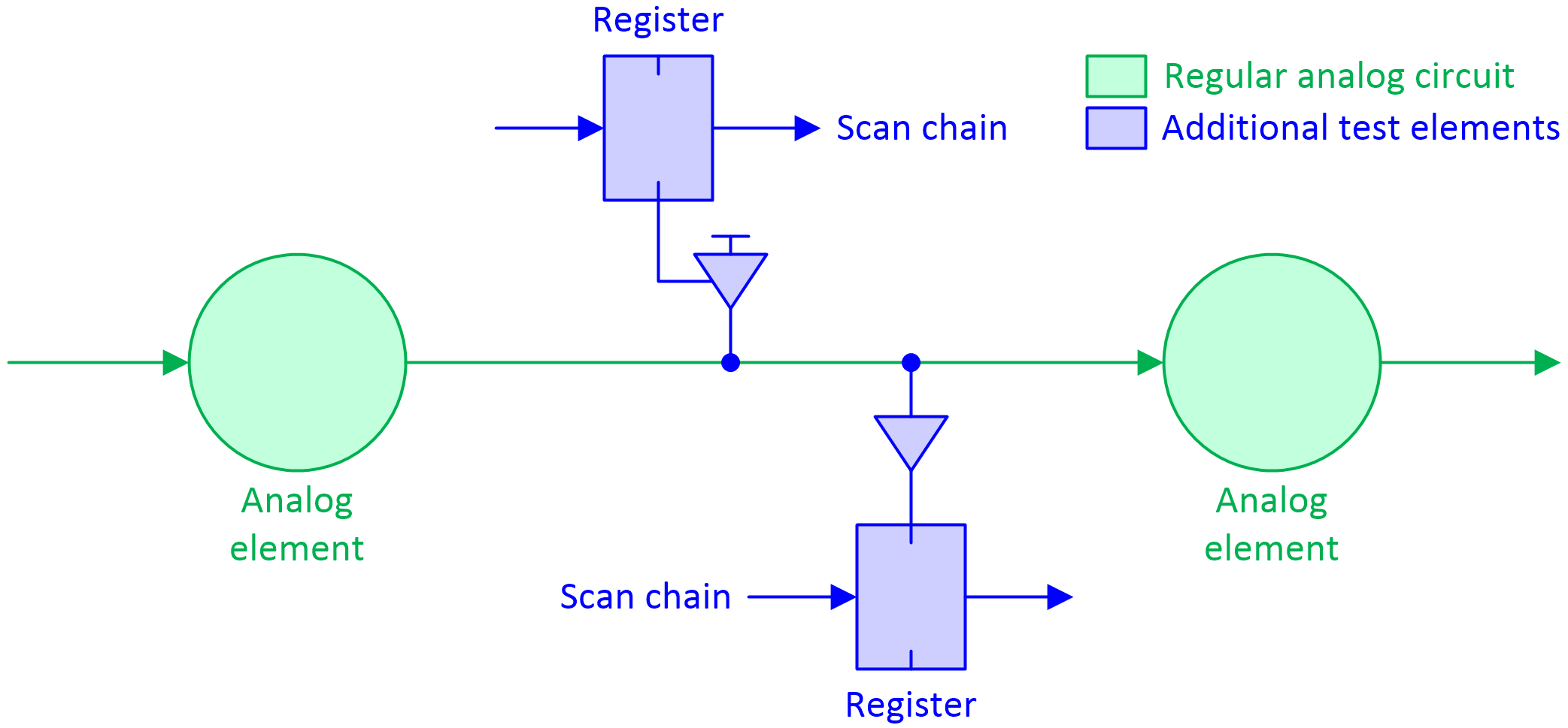
High-level view of inserting and monitoring signals (Source: Max Maxfield)
The regular analog circuit elements and wires are shown in green. The additional test elements and wires are shown in blue. Assume that the analog circuit is placed into some default static (unchanging) state. Now consider the buffer driving a signal onto the analog wire. Based on the 0 or 1 in its associated register element, this can be placed in a tristate condition, thereby having no effect on the circuit. Alternatively, it can be used to overdrive the value coming out of the analog element to a specified voltage. Only one register-buffer combo is shown here, but multiple such combos can be used to inject various voltage values onto the same node.
Similarly, the buffer monitoring the analog wire can be configured to generate a 0 or 1 depending on a specified threshold value, and it’s this 0 or 1 that will be loaded into its associated register. Once again, only one buffer-register combo is shown here, but multiple such combos can be used to detect various voltage (threshold) values.
It isn’t necessary to have both (or either) of these test elements associated with every signal in the analog circuit. Tessent AnalogTest can automatically determine the optimal number and placements required to provide the desired coverage.
All this has ramifications on multiple levels. For example, Etienne provided an example of a traditional analog functional test that took ~20ms to provide ~52% defect coverage. By comparison, using Tessent AnalogTest’s digitally implemented version of an analog structural test took only 76µs to achieve 72% defect coverage.
To be honest, I’m still trying to wrap my head around all of the implications that flow from this new technology, not least that digital verification engineers now have the ability to verify the analog portions of an ASIC/ASSP/SoC without causing their brains to leak out of their ears. What say you? As always, I’d love to hear what you think about all of this.

