


Power distribution and clocks are the essential infrastructure of chip design. Since the earliest days of the integrated circuit, power has been distributed on top of the chip through metal traces that are intermixed with the signal traces. Multiple manufacturers are now investigating back-side power distribution, which require through-silicon vias. Meanwhile, clock distribution hasn’t changed much, but Movellus would like to change that with its new, intelligent approach to on-chip clock networks.
Taking one step back, our industry is wedded to synchronous logic design. Although a few design teams have toyed with asynchronous logic design on chips over the years – I recall the AMULET Arm processors developed at the University of Manchester during the 1990s, for example – EDA tools from the big three EDA vendors all have synchronous design baked into their marrow. It’s very hard to use asynchronous logic on chip designs in the modern world if the design tools don’t support it. Consequently, synchronous logic is the design dish du jour. As long as we continue to use synchronous logic, we’re going to need clocks.
Now that we’re putting more than a billion gates on a chip, clock design and on-chip clock distribution are getting very difficult. Maintaining precise clock and edge synchronization from one side of a chip to another is a monumental challenge that isn’t getting any easier. The same is true for clocking on today’s most advanced FPGA designs. Clock distribution and synchronization are inextricably intertwined with timing closure, which becomes ever more difficult with each new chip generation. Clocks are also deeply intertwined with a chip’s power consumption for obvious reasons: routing multi-Gigahertz clocks around a billion-gate chip burns a lot of power and is very sensitive to design margin.
These challenges are rooted in the way we generate and distribute on-chip clocks. Generally, but not always, one master PLL generates the main clock, and all the other clocks on a chip are derived from the master clock. These clocks are then distributed to every on-chip flip-flop through a clock tree or mesh network. With hundreds of millions or billions of flip-flops on the chip, that’s a lot of high-frequency signal routing that needs to find its way throughout the chip. To maintain close clock synchronization and aid timing closure, the place-and-route software must match trace lengths of the clock-distribution network all the way to the leaf nodes as closely as possible. This design task just keeps getting harder and harder as chips get bigger and bigger. In fact, timing closure and verification now dominate the chip design cycle and push chip tapeout schedules farther and farther into the future.
Movellus believes it has a better way: “Intelligent Clock Networks,” a term that Movellus has trademarked.
The fundamental idea behind the Intelligent Clock Network is simple and elegant: distribute a low-frequency reference clock with very precise edges around the chip and then generate high-frequency local clocks using “Smart Clock Modules” (SCMs). Figure 1 below illustrates the basic concept.
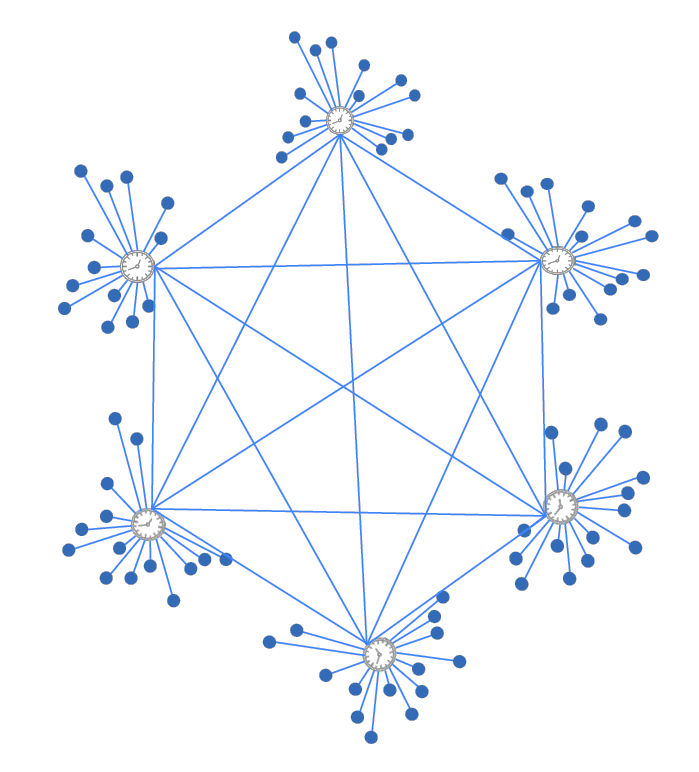
Figure 1: Simplified diagram of the Movellus Intelligent Clock Network. Image credit: Movellus
The Intelligent Clock Network’s central clock-distribution mesh carries the precise, low-frequency reference clock to the SCMs, represented in this graphic by little wall clock symbols. Because there are only a relatively few SCMs on the chip, compared to the millions and millions of flip-flops, it’s much easier to match the distribution mesh’s trace lengths to ensure that the low-frequency reference clock’s edges reach all the SCMs at precisely the same moment. Figure 2 provides additional detail.
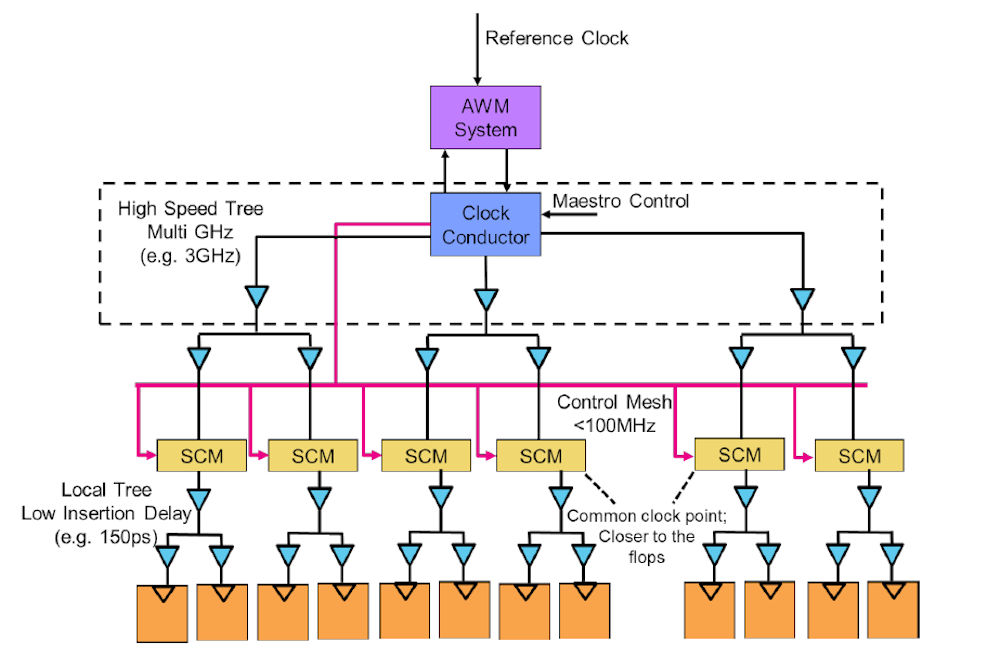
Figure 2: Detailed diagram of the Movellus Intelligent Clock Network. Image credit: Movellus
The high-frequency clocks generated by the SCMs are locked to the precise edges of the low-frequency clock delivered over the main clock distribution mesh. Meanwhile, a simplified high-speed clock tree delivers a “dirty” clock, a clock without precisely controlled edges, to the SCMs for use in generating the precisely synchronized local clocks.
The simple boxes outlining the SCMs belie their complex function. The SCMs do not just generate precise, local, high-frequency clocks from the precise, low-frequency clock edges. They also automatically detect timing changes due to on-chip process variation, aging, and temperature fluctuations. On-chip variation is a growing problem as chip manufacturing enters the so-called angstrom era. Electrical parameters now change noticeably across a chip, and from chip to chip. Temperature changes also cause parametric changes, and all these variations and changes cause on-chip timing to shift unpredictably.
The traditional, static way to deal with all these variations and changes is to enlarge the timing margin at design time, which means throwing performance and power consumption away in exchange for a safer design. This is not a very intelligent way to attack the problem. Movellus’s Intelligent Clock Network IP takes a more, er, intelligent approach. If a path becomes too fast or too slow, the SCM compensates dynamically by inserting the right amount of delay to synchronize its local distribution tree with the clock trees of other SCMs.
Neutralizing the effects of on-chip variation and temperature improves a design’s timing margin. Chip designers can exploit this extra margin in two very important ways. If performance is paramount, designers can become more aggressive with clock frequency, which will make the chip run faster while still allowing timing closure. Movellus claims that the improvement to clock frequency can be as large as 30 percent.
If power consumption is more important for a design, the extra timing margin allows designers to use a lower core operating voltage while holding the clock frequency constant. Because power consumption is proportional to the square of the operating voltage, the lower core voltage can result in significant power savings. Movellus claims that the power savings can be as much as 25 to 30 percent.
The SCMs in the Intelligent Clock Network continue a well-established practice in IC design: adding transistors, which cost very little, to achieve big performance improvements. In this case, the synthesizable SCMs add a relatively few transistors to the IC’s design in exchange for automatically compensating for the effects of on-chip process variation and temperature changes and greatly reducing timing-closure headaches.
No one likes to be the first to try out a new IC technology, in case the technology doesn’t work. The risks are very high for IP pioneers. In this case, the initial chip designs using the Movellus Intelligent Clock Network have already been developed and manufactured. The Movellus Intelligent Clock Network IP has been proven in more than 25 chip designs using more than fifteen different process nodes ranging from 40nm down to 3nm, with a 100 percent success rate.
For example, last year Achronix announced that it had used the Movellus Intelligent Clock Network in its Speedster7t FPGA design, which is manufactured with TSMC’s 7nm process technology. This year, FAST labs, an advanced technology R&D group inside of BAE Systems, signed a deal with Movellus to use its Intelligent Clock Network IP for radiation-hardened chip designs destined to fly into space.
Last month, Movellus announced that it had closed a $23M Series B funding round, which the company will use to expand its R&D efforts and build out its marketing and sales functions. MESH and SK hynix joined existing investors Accelerate Blue Fund, Candou Ventures, Hui Capital, Intel Capital, In-Q-Tel, Michigan Capital Network, Stata Ventures, and other private investors in this Series B round.
The Movellus Intelligent Clock Network looks like a slam-dunk opportunity to me, but you will need to decide whether the incremental cost of the IP is worth it in terms of improved design margin, reduced design time, better performance, and lower power consumption. All these benefits are extremely valuable in chip design.


Seems to me that there’s an underlying false assumption here.
I just don’t believe that there ever will be a design for millions of flip-flops
using the same clock. It is simply beyond human comprehension.
There will have to be a modular design that uses that many. And the tool chains
are not able to handle modularity. So sad, because modularity is absolutely needed.
There are no false assumptions in this article, Karl Stevens. The nodes in Figure 1 and the SCMs in Figure 2 are all digital PLLs capable of generating whatever frequency is needed at that node. The same use of multiple PLLs as clock generators is standard practice on large ASICs. Movellus claims its digital PLLs are significantly smaller than analog PLLs, a claim to be judged by the ASIC design team, looking at IP versus IP.