


My poor old noggin is currently spinning like a top. I was just chatting with Shakeel Peera, who is VP of Marketing, Strategy, and Business Operations for the FPGA business unit at Microchip Technology.
The first piece of intelligence that blew my mind was the fact that the FPGA business unit is one of 23 business units inside Microchip. Give me strength. I remember when Microchip started as a relatively small spin-off from General Instrument (GI) in the late 1980s. Now it’s grown into a multi-billion-dollar behemoth.
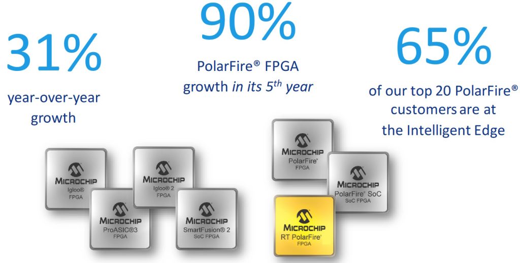
One of Microchip’s claims to FPGA fame is power efficiency, which has powered (no pun intended) their 31% growth over the past year. Of particular interest for me is the PolarFire family. Typically, an FPGA family will start plateauing around its sixth or seventh year, but PolarFire devices—which are now in their fifth year—managed 90% growth last year, and they probably won’t be plateauing anytime in the near future. I’m sure this growth is related to the hard RISC-V processor cores that were introduced in PolarFire SoC FPGAs in 2020. I’m also sure that the availability of RISC-V-based PolarFire SoC FPGAs explains why 65% of Microchip’s top 20 PolarFire customers can be found beavering away at the Intelligent Edge.
Although mega-AI applications like ChatGPT are tied to data centers and the cloud, especially with respect to training generative AI models with a trillion+ parameters, the place to see and be seen is increasingly to be found at the Intelligent Edge. It seems like everyone who is anyone is moving to the edge in terms of where data will be generated and processed. For example, Gartner predicts that 75% of enterprise-generated data will be created and processed outside of a centralized data center or cloud by 2025, which is just two short years away as I pen these words.
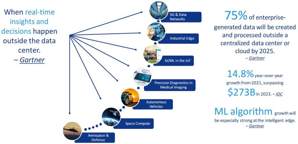
Everyone is moving intelligence to the edge (Source: Microchip)
There are various processing platforms available, including MPUs, MCUs, and GPUs, along with emerging vector processing units (VPUs), and—of course—FPGAs. Of all these, FPGAs distinguish themselves by their reprogrammable nature that allows them to support diverse architectures on the fly. Whenever there is chaos and whenever there is churn in the industry in terms of diversity of SKUs, diversity of applications, and diversity of standards, there is need to be constantly evolving algorithms, and FPGAs are awesome in this regard. Similarly, whenever there is a highly specialized application that needs acceleration at the highest GOPS per watt, FPGAs are awesome at parallel processing.
So, what are typical characteristics of systems destined to spend their days at the edge? Well, they may be deployed anywhere from the smart home to remote areas. They’re usually small, they’re usually real-estate constrained, they’re usually power constrained, and they’re usually thermally constrained. Just for giggles and grins, designers are constrained by what they can do in terms of heat mitigation (no heat sinks, no fans, minimal airflow).
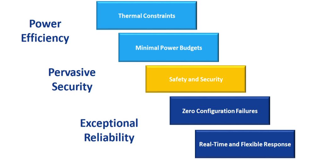
The top five demands of the intelligent edge (Source: Microchip)
Then we have the need for pervasive security, which is intimately related to industrial safety, to public safety, and to nation-state safety (you don’t want your country’s power grid to be hacked into, for example). Last, but certainly not least, there’s an increasing demand for exceptional reliability.
One key aspect with respect to FPGA power consumption is the underlying configuration cell technology. Most FPGA vendors employ volatile SRAM-based configuration cells. By comparison, the folks at Microchip have opted for nonvolatile configuration cell technology. They started with antifuse technology and later moved to Flash. More recently, their PolarFire devices are Silicon-Oxide-Nitride-Oxide-Silicon (SONOS)-based. The results speak for themselves.
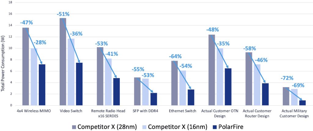
PolarFire designs consume significantly less power (Source: Microchip)
Here we see the same designs implemented on a 28nm PolarFire FPGA versus 28nm planar and 16nm FinFET-based competitor devices. The PolarFire’s Static power is 62% lower than the closest (16nm) competitor while transceiver power is 50% lower than the closest (16nm) competitor.
The 50% lower transceiver power caught my eye. I know how much the other FPGA vendors set store by their transceiver technologies. Shakeel explained this as follows: “Our two biggest competitors conceptually build the Mercedes-Benz of FPGAs while we build the Toyota Corolla. In the case of transceivers, our competitors start off by building very large, very power-hungry functions and then they ‘waterfall them down’ to lower baud rates. But we design and optimize our circuits for these mid-range baud rates from the get-go.”
“When you put all this stuff together, we beat our competition like a drum” (Shakeel concluded, modestly).
As another example, consider the two forward-looking infrared (FLIR) images below. These are from two devices running the same design. The image on the left is the competitor device. On the right we see the PolarFire FPGA.
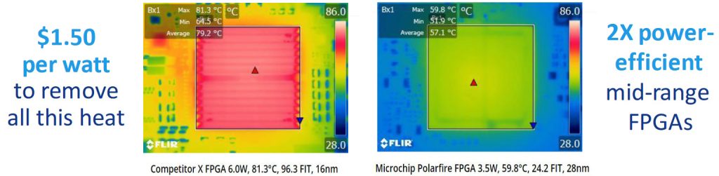
Power is money (Source: Microchip)
When it comes to security, Shakeel notes that everyone talks about cybersecurity, and cybersecurity is certainly important, but data security and design security are meaningless without physical security of the hardware. In the case of the security pyramid illustrated below, for example, the top two layers are where you’ll see most security mitigations taking place, but none of this matters if you don’t have secure hardware.
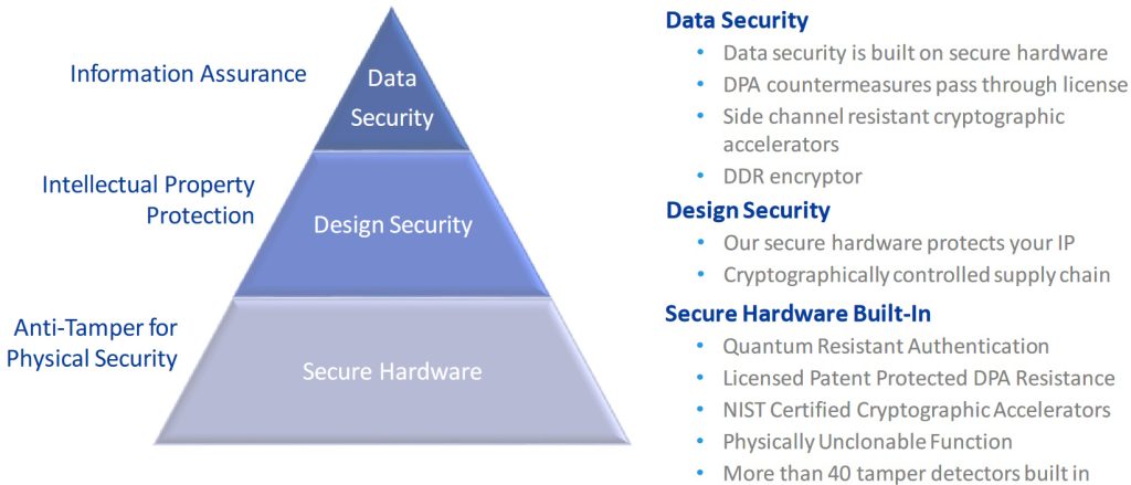
There is no cybersecurity without physical security (Source: Microchip)
PolarFire FPGAs and SoC FPGAs address all layers of the security pyramid, including more than 40 tamper detectors built into the hardware.
I started my career as a member of a team designing CPUs for mainframe computers, so—as you might imagine—I was particularly interested in the hard processor subsystem. Shakeel notes that there were several overwhelming considerations with respect to PolarFire’s processor implementation. First, they wanted to minimize the number of transistors—less transistors means less leakage means less power. If you think in terms of Arm offerings, they wanted to provide the equivalent of a heterogeneous compute environment with A-class processing, M-class processing, and real-time processing, all without having to have separate A-class processors, M-class processors, and R-class processors.
Using the RISC-V open-source ISA allowed the folks at Microchip to build something to their own specification without having to pay a huge architectural license and a development fee to customize someone else’s offering. The result is illustrated below, with five 64-bit RISC-V cores—a real-time monitor core on the left, and a cluster of four 64-bit workhorse cores on the right.
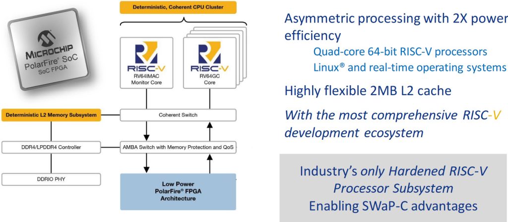
High-level block diagram of PolarFire SoC FPGA (Source: Microchip)
Also included with the processor cores is a memory management unit (MMU), which is required to run an operating system like Linux. There’s a cache coherent switch along with a DDR memory controller that is fully configurable through a standard register stack (speeds, feeds, number of bits, page modes, hashing algorithms, etc.).
There’s so much more we could talk about. For example, computer engineers, system engineers, and software developers outnumber FPGA designers by 100 to 1 (and that’s being generous). These guys think in terms of programming languages like C and C++; they know nothing of VHDL and Verilog. Thus, Microchip’s FPGA development environment includes a High-Level Synthesis (HLS) capability.
This is probably the point where I should note that Microchip FPGAs Speed Intelligent Edge Designs and Reduce Development Cost and Risk with Tailored PolarFire FPGA and SoC Solution Stacks (Ten collections—spanning the industrial and communications sectors and smart embedded vision, motor control and optical access technologies—feature IP, reference designs, development kits, application notes, demo guides, and more), but you can learn all about that by clicking on the link above.
Something else of interest is Microchip’s VectorBlox Accelerator Software Development kit (SDK) for PolarFire FPGAs. This SDK contains different tools that compile a neural network description from frameworks like TensorFlow and ONNX into a Binary Large Object (BLOB). These BLOBs are stored in Flash and loaded into the DDR memory during execution.
As a tempting teaser, Shakeel closed our chat by informing me that he couldn’t really tell me much about Microchip’s forthcoming second generation of PolarFire devices except that they were going to be named PolarFire 2. (On the one hand, adding a ‘2’ may not seem to be overly inspired. On the other hand, if you’ve got a name that works, like PolarFire, sticking with it is a good idea.) I responded that Shakeel hadn’t told me anything, so he relented and said that the new devices will have 2X the power efficiency, 3X the CoreMark score, 13X the TOPS, and 20X the 8-bit inferencing capability.
I will, of course, be reporting further when these bodacious beauties leap onto the center of the stage with a fanfare of Sarrusophones (once heard, never forgotten). Until that frabjous day, I’d be interested to hear what you think about all of this.


Where’s the Beef? This sounds like Blue Sky.
And by the way, tools to build and debug this contraption do not exist.
Which contraption are we talking about?