

It isn’t often that we see an innovation that is really a game-changer. Most of the announcements we get from technology companies, particularly in areas like design-for-test (DFT), have been relatively stable for decades. Normally, we get incremental, evolutionary improvements in technology that yield modest gains in productivity, efficiency, or some other metric. Over time, these improvements add up, and we are able to continue happily along the path of Moore’s Law’s exponential curve.
This is not one of those times.
Mentor has just rolled out their new Tessent Streaming Scan Network and… DFT will probably never be the same. The new technology should significantly reduce the effort, cost, and risk associated with designing-in DFT circuitry into our chips, and it brings a new design process flow that allows us to configure and tune the test process far later in the design cycle than was previously possible, which should be welcome news for many IC design teams for whom test has become a major design headache.
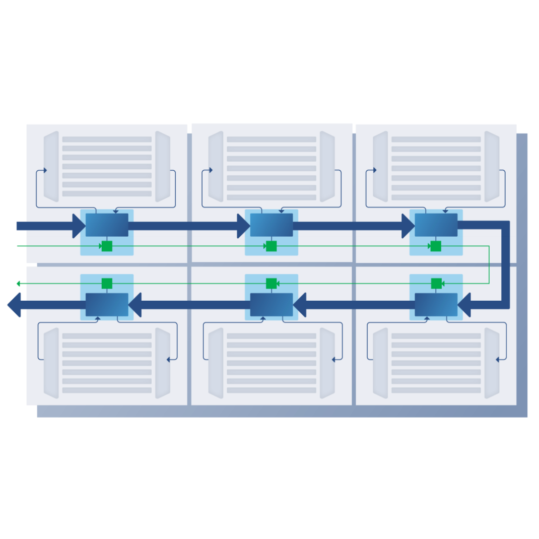
To understand what’s going on with the Tessent Streaming Scan Network, we should start with the current state-of-the-art in on-chip test networks. Since way back in the days when our ancient ancestors returned to their caves, stood their clubs in the corner, rubbed a couple of sticks together to make a fire, and sat down to design their scan networks – things have been about the same. A certain number of pins on the chip (not nearly enough, of course) were designated for test, and our ancestors had to make do with those. They’d fan the inputs out to the blocks that needed to be tested, do some rough calculations on what should be tested when, multiplex the outputs of those chains so they could get the results out of not-enough-output-pins, carve the resulting scan network in stone on the cave wall, and pray to ancient gods that what came out after tape-out would be sufficient to test the chip in a reasonable time.
What Mentor has done is to build a smart, flexible, runtime-programmable scan network to replace the traditional carved-in-stone implementation. They created a bus for test data that loops through your entire chip. That bus carries packetized test data to and from each core under test, and it can be any width you need – even 1 bit. For each of your cores/blocks that needs to be tested, there is a programmable host node attached to the SSN bus that serves and manages the testing of that block. This effectively de-couples the core-level and chip-level DFT. More importantly, it allows decisions and changes to the testing strategy to be made after the chip is fabricated, rather than prior to tape-out. This factor alone is enormous, as we are accustomed to being stuck with whatever decisions we made about test strategy prior to tapeout.
Because the test data is packetized, there need not be any correlation between the width of data required to test each block and the width of the bus; the block’s test monitor can pull data from the bus, buffer and construct the correct width vector for the block, and then clock the data in for testing. This allows the bus to be effectively 100% utilized as (unlike the conventional architecture) there are no large idle periods where input paths are unused. This packing of the bus and resulting optimization of IO pin utilization means a significant reduction in test time – Mentor estimates “up to 4x test time and volume reduction.” And all those muxes that you used to have handling the test output… gone.
The generic and regular nature of the on-chip bus/monitor SSN architecture also makes timing closure and layout simpler and more straightforward. Identical blocks can 100% share testing strategies, with each instance having identical testing cost. Mentor says the architecture also supports tile-based design with abutment, further simplifying layout.
Testing time can also be optimized by throttling the testing of lower-demand blocks in favor of higher-demand ones. This allows optimization of resource utilization and resulting reduction in test time. Intel compared SSN with their own STF as well as traditional mux-based structure and concluded that “SSN was found to reduce the test data volume by 36% and 43%, respectively. It reduced test cycles by 16% and 43%, respectively. Steps in the design and re-targetingflow were between 10x – 20x faster with SSN compared to STF.”
Those are some pretty compelling results.
More difficult to benchmark, but perhaps equally important, is the ability to design and re-design the test strategy after chips are fabricated. There are a number of factors that are very difficult to predict (such as power consumption) that can have a significant impact on the efficacy of a test strategy. With the traditional mux-based architecture, and with the test strategy essentially locked in at tapeout, your ability to make changes after the fact is very limited. This also means you don’t have your DFT design process holding up tapeout for the rest of the team. In many cases, that can result in an earlier and higher-confidence tapeout.
Like many revolutionary improvements, the Tessent Streaming Scan Network will require a bit of change to design flows, project strategies, and mindset. In many cases, such changes slow the adoption of new technologies into the relatively conservative IC design flow. But the benefits of Tessent SSN are compelling enough, and the changes docile enough, that we don’t anticipate that being any significant barrier to adoption.
It will be interesting to watch this methodology evolve. Clearly there are opportunities for optimizing the bus and management, working with high-speed serial IO, and fleshing out the development and analysis tools to robustly support this new methodology. But our take is that this is one of the most exciting changes to hit the DFT space in quite awhile.


