

Just to put you out of your suspense, the tantalizing topic of this column is that a company called PulseForge has developed a technology that allows us to solder surface-mount components onto conductive inks pads and tracks which are themselves printed on thin, flexible polymer (plastic) substrates. This is quite a trick when we remember that the melting point of lead-free solder is around 227°C ± a dibble and a dab, while the maximum working temperature of many low-cost, lightweight polymers is typically around 150°C. Based on these numbers, it would seem that the idea of melting metal (solder) on plastic (substrate) without melting the plastic itself is a bit beyond the bounds of what’s possible. I wonder how it’s done…
As an aside, you might be surprised how long and hard I occasionally agonize over the titles to some of my columns. In the case of today’s offering, for example, I was tempted to make mention of something like “Amazing New Technology for Creating Electronic Circuits!” As true as that would be, however, it really doesn’t set my juices flowing.
It may just be me, but when I see something like “Melting Metal on Plastic Without Melting the Plastic” I immediately think, “Hmm, that sounds like it could provide an amazing new technology for creating electronic circuits!”
One of the great things about being a member of the EEJournal team is that ideas bounce back and forth between us. For example, sometimes when I interview a company and then write and publish a column, I’ll drop an email to Amelia Dalton who runs our Fish Fry Podcast suggesting that the person which whom I spoke—along with the technology we spoke about—would make a great guest-topic-combo for a future Fish Fry episode.
Contrariwise, things sometimes work the other way around. A few weeks ago, for example, Amelia emailed me to say, “Hi Max, I recently did an interview with Stan Farnsworth at PulseForge. Check out my PulseForge Fish Fry. I think they would be a good fit for an editorial piece on EEJournal.”
Well, to cut a long story short (which is unusual for me because I usually do things the other way), I reached out to Stan, who is CMO at PulseForge, and we had a jolly interesting chat that resulted in me squealing “Ooh! Shiny!” (Fortunately, I was using my “inside-my-head voice.”)

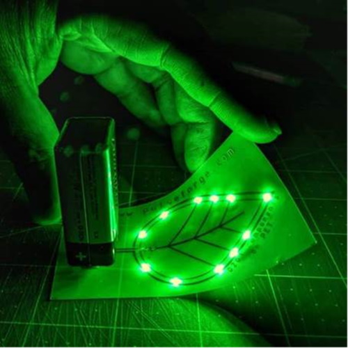
Surface-mount LEDs soldered onto conductive ink printed on thin, flexible plastic substrate (Image source: PulseForge)
Knowing that the current claim to fame of the folks at PulseForge is their aforementioned ability to melt metal on plastic without melting the plastic, and also knowing that the company has been in business for 23 years, my first question was why, 23 years ago, did someone feel moved to say to themselves, “I really wish we could melt metal on plastic without melting the plastic.” Not surprisingly, it turns out that this wasn’t the way things came to be.
A railgun is a linear motor device, typically designed as a weapon, that uses electromagnetic force to launch high velocity projectiles. Deep in the mists of time we used to call the 1990s, the guys and gals who would one day don the undergarments of authority and stride the corridors of power at PulseForge were part of a railgun research group working for the US Defense Department.
This work involved storing vast amounts of energy in a warehouse full of room-sized capacitors, and then discharging this energy into the railgun. In order to initiate the arc, a piece of aluminum foil was used to short the two copper rails at the backend of the gun, with the payload mounted just in front of the foil. When the capacitors were discharged, the aluminum foil was vaporized into a plasma while the payload was accelerated to around 8 kilometers per second by the time it reached the end of the 15- to 20-foot copper rails. A side effect of all this with respect to the aluminum plasma was to create a nanoparticle residue.
So, in 1999, the intrepid team did what any of us would have done, which was to form a company whose mission in life was to commercialize the creation of nanomaterials in the form of nanopowders. After thinking long and hard, they selected “Nanomaterials” as their company name. For reasons too tortuous to go into here, they later changed their name to NovaCentrix, which subsequently spawned PulseForge.
As another aside, the term “deep tech” or “deep technology” refers to those startups whose business model is based on high tech innovation in engineering or in significant scientific advances (this is the opposite of “shallow tech”). The reason I mention this here is that NovaCentrix and PulseForge would both be epitomes of deep tech companies as far as I’m concerned.
However, I fear we’ve jumped ahead of ourselves. Returning to the company Nanomaterials as was, their initial focus was on nanopowder incarnations of metals (e.g., aluminum, copper, silver, gold) and metal oxides (e.g., aluminum oxide, zirconium oxide, titanium oxide). It turns out that nanopowders have myriad uses, including being added to other materials to change the physical characteristics and properties of those materials.
However, there was a fly in the soup and an elephant in the room (I never metaphor I didn’t like). It turns out that nanopowders are tricky little rascals to work with, not least that—being so small—they have a lot of surface energy and tend top stick (clump) together. Thus, if given a choice, rather than be provided with the nanoparticles in powder form, many users desired dispersions employing complex chemistries to keep the particles separate from each other and suspended in a solvent (water, alcohol, etc.). Take silver nanopowder, whose particles have 10X the density of water. The requirement is to achieve neutral buoyancy. The term “ligand” refers to an ion or molecule (functional group) that binds to a central metal atom (or nanopowder particle) to form a coordination complex. Think of attaching airbags to a block of iron to make it float. The same effect can be achieved with silver nanopowder particles using combinations of appropriate ligands and other chemistries. In fact, each nanopowder may be provided in a variety of dispersions (solvents, ligands, and other chemistries) depending on the target customer and application.
Have you ever noticed how customers are never satisfied (bless their little cotton socks)? The next thing the little scamps requested was to modify the chemistry of the dispersions to create conductive inks that could be used to implement additive manufacturing technologies using inkjet printers or screen-printing processes.
Additive manufacturing technologies make a lot of sense environmentally and ecologically speaking. Also, the ability to print things like this can vastly reduce the complexity of the supply chain. All of this makes a lot of sense now, but everything was new 20 years ago. As a result, the folks at NovaCentrix found themselves at the point where everything converged.
OK, we’re closing in on the crux of our conversation. Remember that nanopowder materials in the form of dispersions can be used for a tremendous range of applications, but our interest (for the moment) is conductive inks printed on plastic substrates to be used to create products like medical sensors or conformal displays. In this case, at the end of the day, once the ink has been deposited on the surface of the plastic, our goals are to remove the extraneous chemistry (leaving only the metal) and to then sinter the particles to join them together. The problem is that the temperatures required to perform both these actions are not compatible with the plastic, which is the target substrate.
It was at this point that NovaCentrix, which produces the materials, spawned PulseForge, which forges them as required. In order to do this, the folks at PulseForge returned to their roots, using banks of capacitors to power pulses from xenon flash lamps. In this case, the power is so high, and the output pulses from the flash lamps are so intense, that they act as a heat source.
Now, this is the clever bit. Different materials will absorb, reflect, and transmit light/heat in different ways. Metals are good at absorbing it; plastics aren’t (which is good because that’s what we want). The trick is to use the wavelengths and power and duration of the pulses to get the metal above the temperature where it melts while keeping the plastic below the temperature where it sustains damage. Against all the odds, it turns out that plastics are the ideal substrate for this process, which is completely wackadoodle when you come to think about it.
But wait, there’s more, because the next step is to attach surface-mount components onto the conductive traces. One solution is to use electrically conductive adhesives, but there are limitations to what can be achieved with these materials. What is really required is the ability to work with regular lead-free solder paste.
“What about using a laser to melt the solder paste under the components’ pins?” I hear you cry. I’m glad to see you are (a) paying attention and (b) thinking ahead. Lasers are great. I love lasers. I wonlt hear a word said against lasers, except… The problem with a laser is that you can melt the solder associated with only one component pin at a time. Think about the way a reflow oven works. All of the components are placed on their solder-paste covered pads and the entire board is heated up. When the solder melts, surface tension causes the components to self-align. You’re not going to get that with a laser.
The guys and gals at PulseForge realized they could take the same physics they were already using to dry, evaporate, sinter, melt, or anneal, and they could reconfigure the power delivery to melt the solder on all the pins (thereby allowing the components to self-align).
So, that’s the current state of play. Now that they have this technology up and running, the chaps and chapesses at PulseForge are on a mission to spread the good word to members of more traditional electronic manufacturing communities, letting them know that it’s now possible to melt solder on plastic without melting the plastic because everything happens so fast that the plastic doesn’t mind and the solder doesn’t know. I for one am jolly excited by the possibilities presented by this technology. What say you?


