


Dave Ditzel has a legendary history with computing and microprocessors. He joined AT&T Bell Labs to work on C language development. While there, he developed several generations of processors designed to execute optimized compiled C programs including CRISP, Bell Labs’s “C-language Reduced Instruction Set Processor.”
At Bell Labs, Ditzel also co-authored the foundational RISC document, “The Case for the Reduced Instruction Set Computer,” with UC Berkeley’s Professor David Patterson. Ditzel then joined Sun Microsystems as CTO of the SPARC Technology Business, where he led development of the SPARC RISC processor architecture and the 64-bit SPARC ISA. Oracle bought Sun Microsystems in 2010 and later discontinued corporate SPARC development in 2016. But thanks to SPARC International, the SPARC ISA continues, as fully open, non-proprietary, royalty-free IP.
Ditzel founded microprocessor maker Transmeta in 1995 with the intent of developing VLIW (very long instruction word) processors that fully emulated the x86 ISA using dynamic binary-translation software. This software wrapper converted x86 instructions into VLIW machine instructions on the fly. Transmeta launched its first product, the Crusoe processor, with an elaborate press event at the Villa Montalvo Arts Center in the hills above tony Saratoga, California on January 19, 2000. I was there as a member of the press.
Transmeta positioned Crusoe as a low-power alternative to Intel and AMD x86 offerings for thin-and-light notebooks and other mobile devices. The company’s processor sales looked promising, initially. It seemed that Transmeta had carved out a seemingly protected niche – low-power x86 processors for battery-powered devices – while AMD and Intel tangled with each other on the high-performance, high-power x86 front.
But Crusoe’s sales and press coverage gave Intel a sense of how desperately the thin-and-light laptop and mobile markets wanted a low-power x86 microprocessor. Intel then moved quickly to fill the Transmeta-sized gap in its x86 processor product line with an “almost-good-enough” reduced-power die shrink of the Pentium III processor, dubbed the Pentium III-M. Intel then quickly followed the Pentium III-M processor with the Pentium M. The “M” is for “mobile,” of course.
Transmeta’s Crusoe processor delivered lukewarm application performance, so Transmeta doubled the VLIW instruction width from 128 to 256 bits for its second-generation Efficeon processor, which ran x86 code faster than Crusoe. However, at the same time, fabless Transmeta switched foundries and subsequently ran into trouble with delivery schedules. By 2007, the company had shifted its business model to IP licensing. Transmeta was acquired in 2009, and operations closed down later that same year. Exit Transmeta from the processor wars. Sic transit gloria mundi.
All this is prologue, proving that Dave Ditzel is no stranger to microprocessors, to thinking big, and to thinking well outside of the box. His latest venture is Esperanto Technologies, and he’s still operating way outside of the microprocessor box.
Ditzel presented details of Esperanto’s ET-SoC-1 ML (machine learning) inference chip at Hot Chips 33 in August. This chip fully displays Ditzel’s long, long association with RISC processors. The ET-SoC-1 ML inference engine incorporates 1092 (that’s “one thousand ninety-two”) customized, 64-bit RISC-V microprocessor cores, 160 Mbytes of on-chip SRAM, and assorted I/O ports – all on one 7nm die.
“Ambitious” is an understated word for this chip design.
As the name implies, the ET-SoC-1 ML inference chip is designed to provide superior power/performance results when executing ML inference workloads. It does this through economical circuit and logic design and specialized, low-voltage power-supply design techniques.
Of the 1092 RISC-V processor cores on the ET-SoC-1 ML chip, 1088 cores are Esperanto’s “ET Minion” cores, an obvious reference to the scads of adorable, loyal, yellow-skinned worker bees in the animated “Despicable Me” movie franchise. The ET Minion cores are based on the open 64-bit RISC-V ISA, with proprietary vector and tensor instruction extensions developed specifically for ML applications. These ISA extensions support single-clock operations on floating-point vectors and tensors as large as 256 bits using 16- or 32-bit operands, and 512 bits of integer data using 8-bit operands.
Fig 1 illustrates the layout of an ET Minion core. As Fig 1 shows, the vector/tensor unit dwarfs its attached 64-bit RISC-V integer controller core:
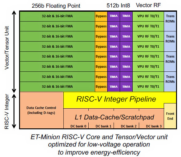
Fig 1: Esperanto’s ET Minion processor core augments a RISC-V processor with a tensor/vector unit that’s more than twice as large as the RISC-V integer unit.
Normally such a vector/tensor unit would be designed as a CPU-hosted accelerator, not integrated directly into a microprocessor IP core. The Google TPU (tensor processing unit) is an example of such an accelerator.
Once Esperanto developed the ET Minion core, the remaining ET-SoC-1 ML inference chip’s design became a step-and-repeat exercise. (Yes, I have just made a gross oversimplification, and you’re about to see why.) The first step-and-repeat operation groups eight of the ET Minion cores and 32 Kbytes of shared instruction cache into “Neighborhoods,” illustrated in Fig 2.
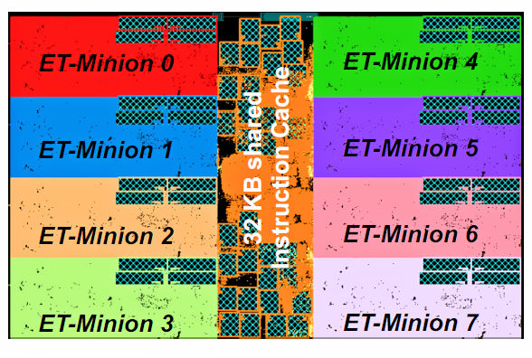
Fig 2: Eight ET Minion processor cores and 32 Kbytes of shared instruction cache RAM comprise an ET-SoC-1 ML inference chip “Neighborhood.”
Four 8-core ET-Minion Neighborhoods are then connected to four on-chip, 1Mbyte SRAM banks through a 4×4 crosspoint switch to form a “Minion Shire.” (The Esperanto naming committee must have had a field day with these names.) A Minion Shire block diagram appears in Fig 3.
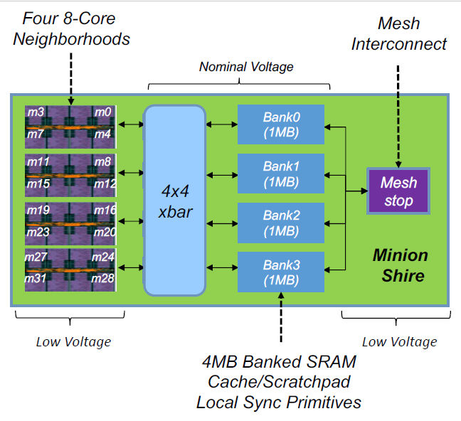
Fig 3: Four Neighborhoods with four 1-Mbyte SRAM banks and a NoC interface constitute a Minion Shire on the ET-SoC-1 ML inference engine.
The Minion Shire’s four 1Mbyte SRAM banks can be configured as cache or as scratchpad RAM, depending on the needs of the ML application. The four SRAM banks also connect to a “Mesh Stop,” which serves as the Minion Shire’s on-ramp to the ET-SoC-1 ML inference engine’s internal NoC (network on chip).
The full ET-SoC-1 ML inference engine die layout consists of 34 Minion Shires, with some additional Shire types including a Shire that incorporates four high-performance Esperanto Maxion processor cores (also based on the RISC-V processor core), eight Memory Shires (each containing an LPDDR4 SDRAM controller), and a PCIe Shire. All Shires incorporate Mesh Stops and communicate with each other through the NoC. Fig 4 provides a diagram of the entire ET-SoC-1 ML inference engine die layout.
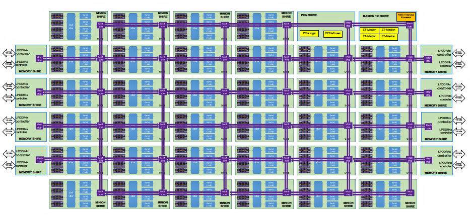
Fig 4: The full ET-SoC-1 ML inference engine consists of 34 Minion Shires, a quad-core ET Maxion processor Shire, eight Memory Shires with LPDDR4 SDRAM controllers, and a PCIe Shire.
Esperanto designed the ET-SoC-1 ML inference engine with a 120W power budget in mind. That budget is based on the amount of power available to an open-source Glacier Point v2 board, which was designed for the Open Compute Project’s Yosemite V2 next-generation, multi-node server platform. Esperanto has designed a Dual M.2 module that plugs into the Glacier Point v2 board. This Dual M.2 module combines an ET-SoC-1 ML inference engine with 24 LPDDR4 SDRAMs. The Glacier Point v2 board can accept as many as six of these Dual M.2 modules, creating a plug-in server card with 6,558 RISC-V cores (Minion and Maxion cores) and as much as 192 Gbytes of LPDDR4 SDRAM.
With six ET-SoC-1 ML inference engine chips and associated SDRAM, that 120W power budget works out to 20W per Dual M.2 card. Esperanto needed to hierarchically incorporate low-power features into the ET Minion cores, the Neighborhoods, the Shires, and the NoC, to cram more than 6000 processor cores and associated LPDDR4 SDRAM within the Glacier Point V2 board’s 120W power envelope.
Given the target architecture for the massively parallel ET-SoC-1 ML inference engine, Esperanto analyzed the relationships and dependencies among clock frequency, core power supply voltage, and application performance to find an optimal set point for the 1088 ET Minion processor cores on the inference engine die. The resulting power/performance/voltage curve appears in Fig 5, which shows that the ET Minion processor cores need to run at approximately 0.4 V to deliver maximum performance while meeting the Glacier Point Dual M.2 card’s 20 W power goal. (This number includes the operating power for the LPDDR4 SDRAMs.)
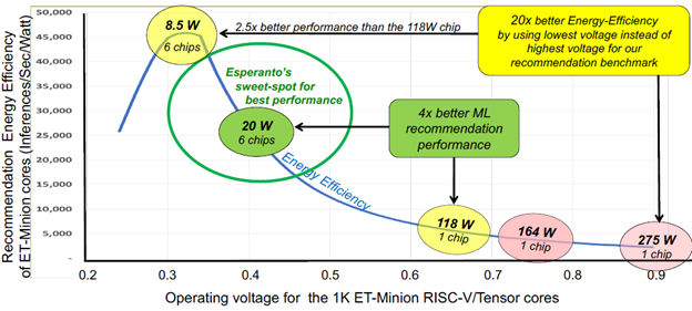
Fig 5: Extensive analysis showed that the ET-SoC-1 ML inference engine would meet its 20W power budget by running the 1088 on-chip ET Minion processor cores at approximately 0.4 V.
During his presentation at Hot Chips 33, Ditzel pointed out that a 0.4 V core operating voltage was neither sub-threshold nor even near-threshold for transistors made with the target 7nm process technology. He claimed that the 0.4 V operating voltage is therefore well within reason.
Based on its analyses, Esperanto claims that the ET-SoC-1 ML inference engine achieves 123X better performance per watt on the MLPerf Deep Learning Recommendation Model benchmark compared to an Intel Xeon Platinum 8380H processor and 25.7X better performance per watt on the ResNet 50 benchmark compared to an Intel Xeon Platinum 9282. These particular Xeon processors were announced by Intel in Q2, 2020 and Q2, 2019 respectively. They don’t represent Intel’s latest Xeon silicon, so get out the salt shaker for these Esperanto claims.
Ditzel’s benchmark numbers were all theoretical at the time of his Hot Chips 33 presentation because Esperanto had just received first silicon for the ET-SoC-1 ML inference engine from the foundry and had not yet had time to get the chip working. Such is the stuff of marketing benchmark comparisons between simulated processors and real silicon. It will be extremely interesting to see if and how reality catches up with Esperanto’s simulation numbers.
It will also be interesting to see if history repeats itself for Dave Ditzel. He once tweaked Intel’s nose with the low-power Transmeta Crusoe x86 processor. Intel responded vigorously to a clear and present danger directed at its processor market and, as a result, Transmeta is no more. The Esperanto ET-SoC-1 ML inference engine is playing another low-power game on a different piece of Intel’s market turf – the data center – which is also currently occupied by opposing teams from AMD, Nvidia, Xilinx, Google Cloud, Amazon Web Services, and several more ML contenders, in addition to Intel.
This will be quite a battle. We’ll be watching to see what happens.


Machine Learning can help automate the drug development process to lessen the burden of repetitive data processing and analysis tasks.