

The upshot: new NIL/SWIL sensing technology from Artilux uses longer-wavelength light, making ToF measurements safer and more accurate.
Cameras flatten us all. We can see what we’re looking at, but there are two limitations: everything is squished into 2D, so that our noses are in the same plane as the front of our ears; and we can’t tell how far away – or how big – something is without other contextual clues (like using a penny for reference). We can solve this using 3D imaging. Lidar is the defining example of using light for ranging.
One common approach is to use time-of-flight (ToF) technology, which uses a laser to send a light pulse that bounces off the target. The reflected signal is received, and the time elapsed between the sent signal and the detection of its reflection determines the distance (modulo the laser pulsing frequency, to distinguish one pulse from the next one).
This is typically done using near-infrared light (NIL), which is less likely to be jammed by all of the visual light that we normally see (more on that in a sec). And silicon is good at detecting NIL – up to a point. And so your typical application has used NIL with wavelengths in the range of 850 to 940 nm.
Sun Spots and Eye Sores
But there are a couple of concerns in this region. First is that whole visible-light thing we just mentioned. It’s not so much about visibility per se; it’s about where the light comes from. In order for ToF to work, you have to know that the light you measure came from your intended source. The sun puts out all kinds of wavelengths, and some of those will compete with the intentional light pulses if you’re trying to image something outdoors.
It turns out that there’s a nice minimum in the sun’s spectrum, and it would be nice to send the pulses at that wavelength, since there won’t be any solar light to confuse things. But that wavelength is above the 940-nm point.
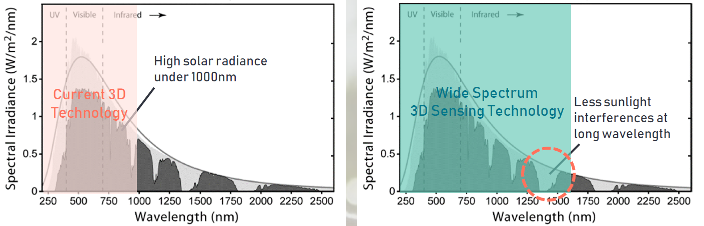
(Click to enlarge. Image courtesy Artilux.)
The second big issue is safety. Normally our eyes react to intense light by closing the iris to restrict the amount of light impinging on the retina. But the iris doesn’t react to these NIL wavelengths, making for a potential eye hazard. That means you need to restrict the power of the laser, which ends up limiting the resolution. Above 1400 nm, however, the retina won’t absorb the light, making this a safer zone. In the diagram below, you see that we’re currently limited to Zone 1, which is unsafe. As told by startup Artilux, Zone 2 is 10-100x safer; Zone 3 is safe. At that point, you’ve departed near-infrared and entered the short-wavelength infrared regime.
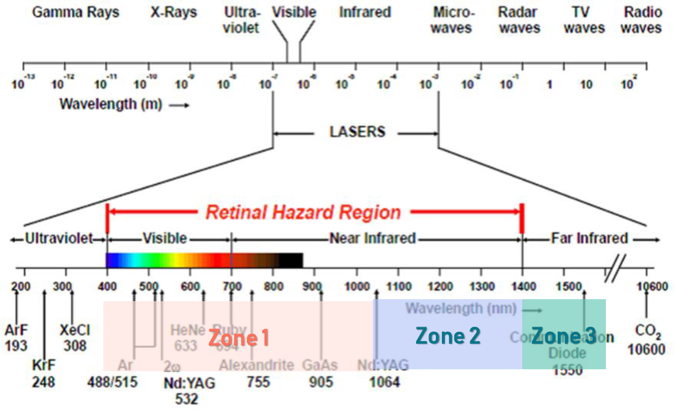
(Click to enlarge. Image courtesy Artilux.)
What’s Old is New: Germanium
So the answer to these concerns is obvious, right? Just use a longer wavelength. The problem is that silicon isn’t good at detecting these longer wavelengths; it’s good for Zone 1. Germanium can detect that light, making both Zones 2 and 3 available, but who wants to build an entire chip out of germanium? That’s so 1940s!
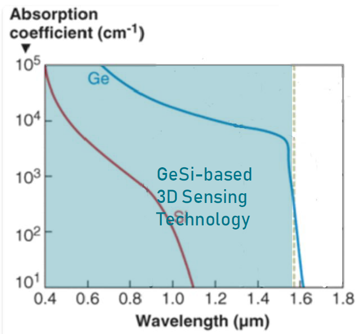
(Image courtesy Artilux.)
That’s the direction Artilux has gone – while still leveraging our basic silicon infrastructure. They’ve built what they call GeSi, which is a layer of germanium deposited onto a silicon wafer. This should not be confused with SiGe, which is silicon doped with germanium as a uniform layer. It also bears noting that we’re talking only about detecting light, not emitting the laser light. III/V materials are still best for lasing – although now we’re talking about tuning them to a different range.
While it sounds simple to deposit Ge over Si, there’s a 4% lattice mismatch. That can cause delamination and thermal stress as the two materials expand at different rates, and there’s a thin defect boundary layer between them. Artilux is not disclosing the specific pixel design that addresses these issues, although they did note that it’s patented. In one of those, “What was I thinking?” moments, I found such a patent for them – and, like most patents, it obfuscates with a bunch of ways you could do it, thereby not really illuminating which of those ways is the one they use commercially.
They can also include a distributed Bragg reflector (DBR) to reject ambient light and limit the admitted light to a 50-nm window. A DBR consists of several alternating layers of materials, and the thickness of the layers determines which light passes through. So the window is tunable to the extent that one chip can set the window one place, while another sets it another place. (It’s not tunable in situ for a given chip.)
Bonding with Silicon
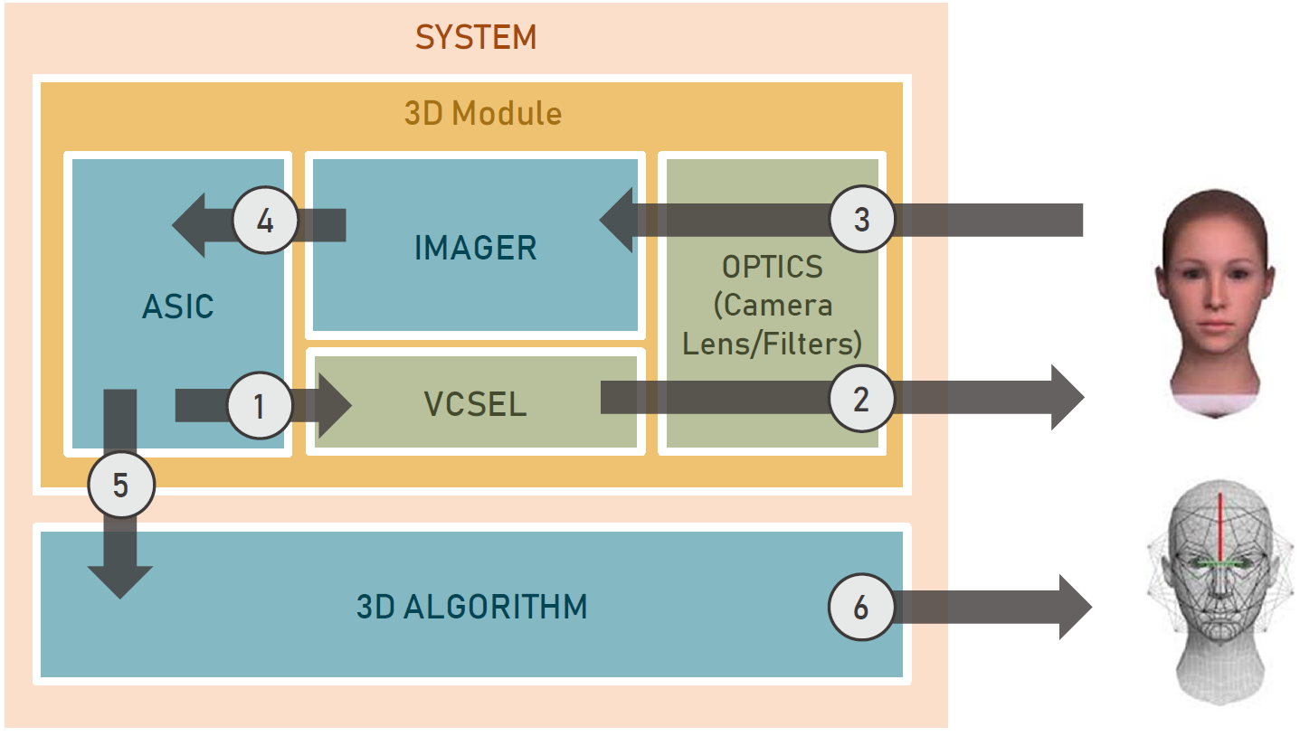
Artilux considers this to be a single “chip” that integrates both the sensing and the SoC that processes the signals. In truth, it’s not a single chip, but two chips bonded at the wafer level. The sensor is illuminated through the back side of its wafer, putting the pixel circuitry inside the bonded pair. The yield is good enough to bond at the wafer level rather than having to assemble with known-good dice.
(Image courtesy Artilux.)
So, with the ability to sense these frequencies within safety zone 3, or even the upper ranges of zone 2, you can use higher laser power, improving the signal-to-noise ratio. And if it works to put the laser into that area of low solar contribution, you can also get a yet better signal. Artilux says that this means better accuracy of the image. They can operate at two frequencies, 100 or 300 MHz. I referred to pulses above, but one of their papers, when presenting the mathematical rationale, refers to this as a sinusoidal signal running at the given frequency; it’s a phase measurement. The higher frequency gives better depth accuracy.
(Image courtesy Artilux.)
Their business model has two ways of bringing this to the market. They’ll have some customers to whom they’ll sell the individual chips, but for others, they’ll offer full modules, saving some design time. These products should be available in January 2020.
More info:
Sourcing credit:
Erik Chen, Co-Founder/CEO, Artilux


What do you think of Artilux’s approach to infrared ranging?