

I was just chatting with the guys and gals at Limata. These clever little scamps specialize in creating affordable laser direct imaging (LDI) solutions for printed circuit boards (PCBs). The exciting news is that they are about to turn the industry on its head because they’ve just introduced the ability to LDI the solder mask — all inks and colors — a feat no one else has previously managed.
Things have certainly changed in the PCB world since I started out as a bright-eyed, bushy-tailed young engineer. In the very early 1980s, the company I worked for owned an automatic wire wrap machine. We would feed it a netlist in the evening and depart for our homes. When we returned in the morning, we either found a prototype board waiting to be tested, or we were presented with the most awful tangle of wires you can imagine.
A few years later, we purchased a workstation whose only task was to facilitate PCB layout. This beast featured two large (for the time) monitors. The first was black-and-white; this is the one we used to enter the commands like “draw a wire from [x1,y1] to [x2,y2].” The second was in color; this is the one that displayed the traces and vias and pads and suchlike.
Suffice it to say that using this beast was painful and time-consuming. Furthermore, any error messages it generated were cryptic, to say the least. I remember it once issuing an error in the form of a string like “E64” flashing in the screen in big letters. We then had to go through a shelf of monstrous manuals to track down the corresponding explanation, which turned out to be “System Overheating,” on this occasion. On the bright side, I have to give credit to the writers of the manual — when we turned round, we discovered that the system was on fire (seriously).
The only thing that made all of this possible is that we were a small company designing relatively small boards with relatively few components and relatively few traces (a.k.a. tracks). The fact that these traces were anywhere from 1/16” to 1/8” wide (or larger) certainly didn’t make things worse.
I think it’s fair to say that the PCB landscape has changed over the years. These days, PCBs have “traces and spaces” (i.e., the tracks and the gaps between adjacent tracks) that are getting smaller all the time. At the time of this writing, traces and spaces of 4 mil and 3 mil are pretty typical in North America, where one mil is equal to one thousandth of an inch (which explains why it’s also referred to as a “thou”). The closest unit to the mil in the metric system is the micrometer (a.k.a. micron), which is equal to one millionth of a meter. Thus, one mil is equal to 25.4 µm.
It is possible to go down to 2 mil lines and spaces in North America, but not all PCB fabricators (a.k.a. “shops”) offer this, and the ones that do will charge you for it. In China, by comparison, it’s possible to go down to 1 mil lines and spaces, but I’m assuming these are small boards like the ones you find in smartphones. The reason I’m assuming this is the deformation and registration problem, but I fear I’m getting ahead of myself…
Conundrums with Contact Imaging
There are myriad possible processes used to create PCBs, such as subtractive (where you remove the unwanted copper to leave the desired traces) versus additive (where you add the copper to form the traces on the bare substrate).
The most common process is to start with a layer of non-conductive substrate — such as FR4 — which is clad with a thin layer of copper. Any required holes are drilled through the board and plated with copper. These include special holes and pads called fiducials, which act as little target registration marks, and which are used by humans or automatic vision systems to align the boards and imaging masks.
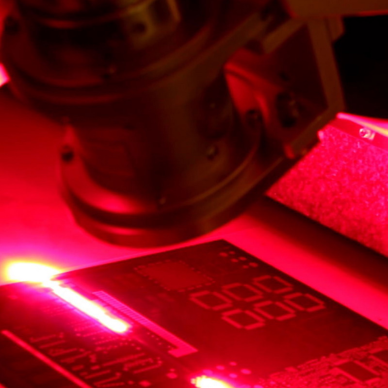
A film of etch resist is applied to the top of the copper. In the case of contact imaging, a 1:1 photographic mask is laid on top of the resist. This is where the fiducials mentioned above are used to make sure everything is aligned.
In the case of a negative-resist process, ultraviolet (UV) light is shone through the transparent areas of the mask to harden the resist over the copper we wish to keep, and then a solvent is used to remove the unwanted resist.
Next, the board is placed in an acid bath, which dissolves any exposed copper not protected by the resist. This process is called “etching” (hence the reason we call the layer of resist “etch resist”). Finally, the board is washed in a solvent that removes any remaining resist. By this means, the pattern in the mask is transferred to a corresponding pattern in the copper.
As an aside, there are also positive resist processes, but we won’t discuss those here. If you are desperate to learn more about all of this, may I humbly suggest (I pride myself on my humility) my book Bebop to the Boolean Boogie (An Unconventional Guide to Electronics) for further reading.
Using this process, applying the UV takes only few seconds. The more time-consuming part is registration — aligning the board and the mask — which can take up to 8 or 10 seconds if performed by hand (this is the case more often than you might think).
Not surprisingly, registration problems get worse as the boards get larger and their traces and spaces get smaller. These problems are only exacerbated by the fact that the boards can expand and contract in response to temperature changes. Even worse, deformations caused by these expansions and contractions can easily be non-linear; that is, different areas of the board can be affected to greater and lesser extents, which can make registration a pain in the nether regions (on a good day) or totally impossible if you are dealing with really fine traces and spaces and the wind isn’t blowing your way. As a result, yield may fall dramatically as the density of the interconnect increases. In some cases, yield may fall as low as 65%, which cannot be a good thing, whichever way you look at it.
Laser Direct Imaging to the Rescue
Now, I’d heard about the concept of Laser Direct Imaging (LDI) way back in the dark ages we used to call the 1990s, but my understanding was that it was way too slow and expensive for real-world production runs. It seems things have changed.
A number of companies started to offer commercial LDI solutions in the early 2000s. They improved the speed by using multiple lasers, but the costs were still high enough to make your eyes water. We’re talking in the order of $700K to $1M per machine. Even worse, these companies would force their customers to agree to a $100K per year service contract.
This is where the folks at Limata (you can also check them out on LinkedIn) enter the picture, because they decided to do things differently. Let’s start with their X1000, which they describe as “A universal and cost-efficient Laser Direct Imaging (LDI) system platform designed for the flexible use in high-mix/low-volume PCB manufacturing environments during the dry-film patterning or solder mask imaging process.”
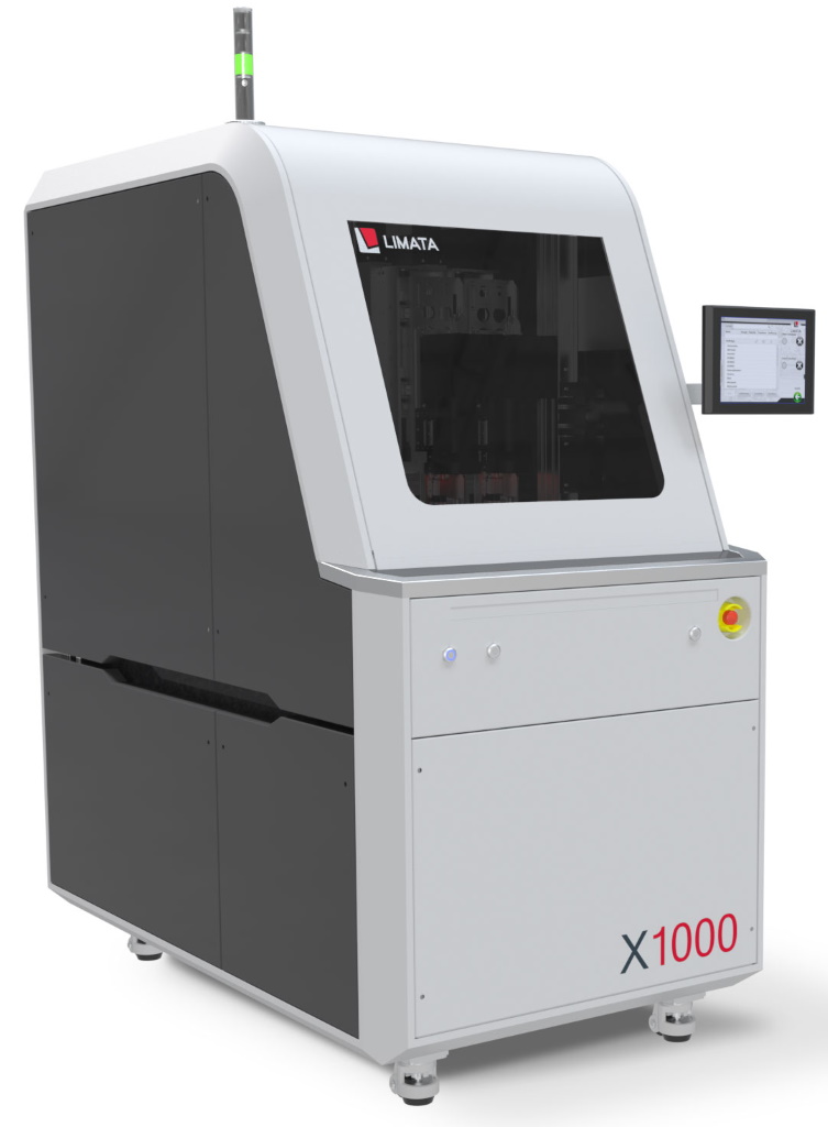
The X1000 Laser Direct Imaging (LDI) PCB System (Image source: Limata)
What we are talking about here is a machine that’s 1 m wide, 1.5 m deep, and weighs in at around 1,000 kg. You can purchase it with between 1 and 4 heads, each containing between 1 and 6 lasers, which (obviously) means you can have between 1 and 24 lasers depending on how fast you want to go.
The great thing here is that you can start off small and add more heads and lasers as required. I’m told a mid-range configuration will cost around $250K to $300K with no forced service contract. And, if you do decide a service contract is a good idea (and who wouldn’t?), we’re talking about really nice service packages that range from only $5K to $10K a year.
Now, here’s where things start to get really interesting (although not as interesting as they are going to get), because registration is fully automatic. Even better, the X1000 automatically detects any distortion (both linear and non-linear) in the board caused by temperature cycling and adjusts the imaging accordingly. One way to think about this is that, unlike the contact imaging process where a single mask is used on every board, this LDI process is like having a unique mask for each board, thereby raising the yield to 100%.
But wait, there’s more, because the X1000 can achieve sub-1 mil lines and spaces, which blows contact imaging out of the water. Even better, the X1000HR (“high resolution”) can achieve a resolution of 8 µm traces (that’s 0.32 mil) that meets the stringent demands of IC substrate and MSAP process production and makes fine line printing affordable for small series production.
And this is only the beginning, because we also have the X1000A for a fully integrated “Island of Automation” or “In-Line” LDI process operation, along with the X2000 and X3000 for those who demand “more” (see the Limata Products Page for more details).
But none of this is what I wanted to talk about…
Introducing LUVIR
I told you things were going to get even more interesting, because the folks at Limata have just announced the availability of something they call LUVIR, which provides LDI for the solder mask stage.
At first, I was a tad underwhelmed to hear this news. “Surely this is a no-brainer,” I thought, but that just goes to show how little I know. It turns out that using LDI on solder mask inks is non-trivial because there are a bunch of different inks with a variety of diverse characteristics. In fact, pretty much the only thing they share in common is the fact that they require 10X to 20X more UV than does the traditional etch-resist LDI step.
This is where we get to look at the name LUVIR a little more closely. The ‘L’ is for Limata, the ‘UV” is for ultraviolet, and the ‘IR’ is for infrared.
It’s long been known that less UV energy is required to cure the solder mask if the solder mask is at a higher temperature. The problem is that heating the entire board takes time (plus it causes the board to expand and distort).
A UV laser provides high precision, but with relatively low energy in the scheme of things. By comparison, an IR laser provides a lot of energy, but with relatively low precision. What the brainiacs at Limata discovered is that, if you heat up the solder mask using an IR laser, then you can use your regular UV laser to complete the hardening process. Furthermore, the IR laser, which tracks a little ahead of the UV laser, heats only a very small area of the board at a time, and only for a very short period of time at that, which means it’s “come and gone” before the underlying board itself has time to react.
The chaps and chapesses at Limata have proven this process with every type of solder mask ink they can lay their hands on. Each type of material requires a slightly different time/temperature and UV/IR treatment, but the folks Limata have compiled a suite of recipes that handle everything for you.
What about the folks who have already purchased X1000, X2000, or X3000 LDI machines? I’m glad you asked — all that is required is for them to swap out the existing UV-only head assembly with a new UV-IR counterpart, after which they are immediately “up and running.”
Personally, I think this is going to be a game-changer. I can easily envisage PCB shops in China and the rest of Asia jumping all over this technology. I only hope that the PCB shops in North America and Europe don’t drop the ball on this one. Speaking of which, if anyone wants to learn more, they can contact Limata’s Founder and CTO, Matthias Nagel, by email (matthias.nagel@limata.de) or phone (+49 89 21 90 91 135) and tell him “Max says Hi.”


As you note, LDI for solder mask has been around for 20 years. Limata makes a low end version of the LDI. Not sure why you chose to focus on them. This is no game changer. Limata’s LUVIR technology actually came out well over a year ago. Moreover, there’s patents on this concept dating back nearly 20 years as well.
It is fun to see that someone hiding behind the synonym PCBguy gives his expertise to a technology, he / she has not really understood. But as well know, this happens always on the web.
First of all, great article Max, by the one hand it is really entertaining to read the introduction with the historical background, by the other hand it summarizes the benefits of Limata’s technology and systems very good.
Now. lets face to the arguments from our PCBguy:
1.) Limata makes low end version of the LDI
As Max stated, just a short look on the reference list of Limata customers of LUVIR technologies shows many of leading PCB suppliers in EU and North America. Now everybody can make his own picture why all these suppliers decided to go with Limata because of their “low end version systems”.
2.) Limata’s LUVIR technology actually came out well over a year ago
Sure, as of today, it is running in many productions worldwide and has demonstrated its stability and efficiency on millions of boards in the industry. It is good to report about a “game changing technology” when you know that it is already approved in the field.
3.) Moreover, there’s patents on this concept dating back nearly 20 years as well
Ouch, completely wrong. Limata has patented this technology worldwide already many years ago.
There is no compatible or similar technology.
Every interested reader should stick to the facts, Max is listing here. These are proven and evidence-based facts and no sensless and anonymous competitor bashing comments. PCBguy2 (guess who we are ;-))