

Prototyping has certainly come a long way since I started my career back in those days of yore that we used to call the 1980s. One of the prototyping techniques we employed was called wire-wrap, which we thought amazing at the time, but which now seems incredibly “clunky” in hindsight.
Wire-wrap was particularly well suited to the sort of designs I was involved with at that time. That is, systems involving large numbers of relatively simple digital logic integrated circuits (ICs). We started with a piece of insulating board that could be several feet square. This board came with an array of pre-drilled holes on a 0.1” pitch. We also had hundreds of special wire wrap IC sockets with long pins.
I think the pins were around 0.75” in length. However long they were, they certainly protruded proudly out of the bottom of the board. We then flipped the board over and used a special wire wrap tool to strip an inch or so of insulation off the end of a piece of wire and wrap the bare wire around one of the pins. Each board could have hundreds or thousands of these point-to-point connections.
I wish I’d thought to take photos of the designs we were working on and the tools we used, but this simply didn’t cross our minds at that time. It wasn’t like now when you can simply whip out your smartphone and click away. I would have had to amble down to the store to purchase a disposable camera containing a roll of 35mm film, then return to the lab to take the pictures (including studies of my thumb). Next, I would need to convey the camera to the local chemist (pharmacist) for them to send it off to be developed, and then wait a week or two before forking out a fortune to see the results of my endeavors. It really didn’t seem worth the effort at the time, but I now regret my lack of foresight with respect to securing my own photographic record of those golden days.
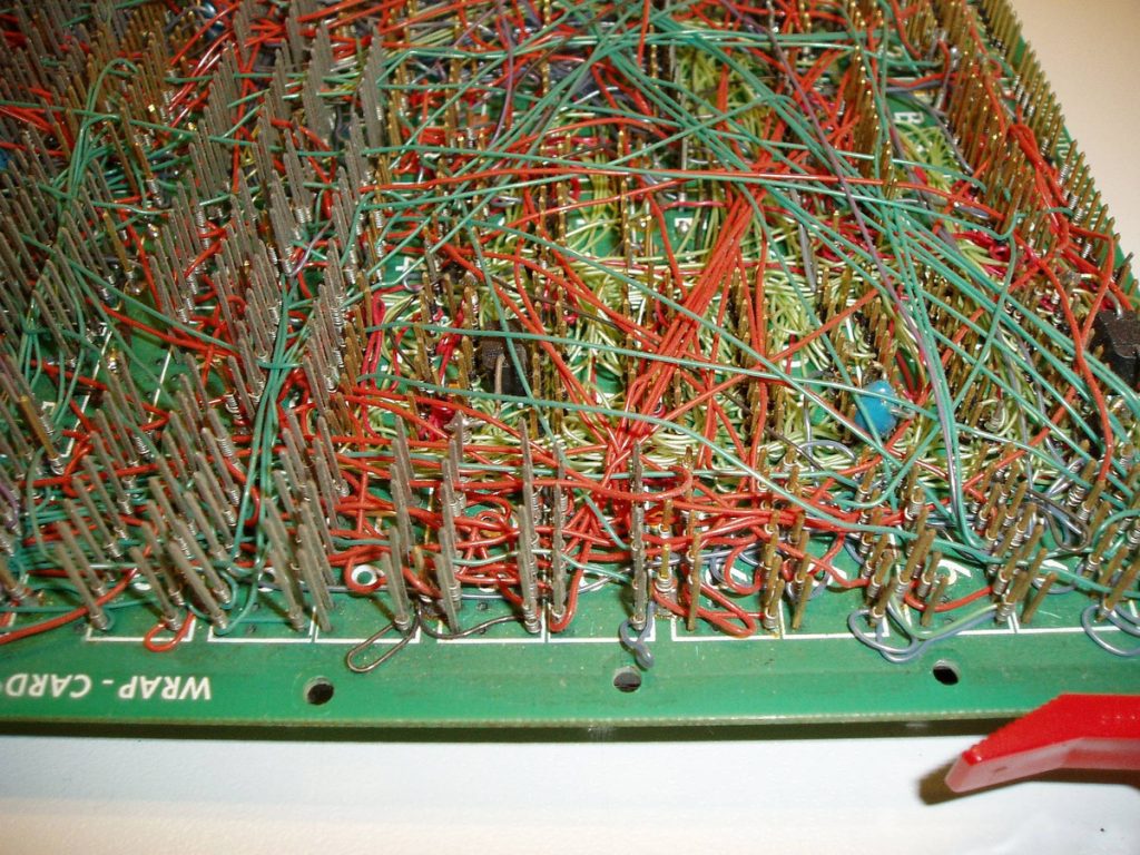
Example of the underside of a wire wrap board (Source: Wikinaut/Wikipedia)
Although wire wrap may seem horrific to the untrained eye, this form of prototyping had several good points, including the ability to quickly make changes, which was jolly useful because it was more than easy to make errors. As the Wikipedia says: “Wire wrap construction can produce assemblies that are more reliable than printed circuits: connections are less prone to fail due to vibration or physical stresses on the base board, and the lack of solder precludes soldering faults such as corrosion, cold joints and dry joints. The connections themselves are firmer and have lower electrical resistance due to cold welding of the wire to the terminal post at the corners.”
At some stage, the small company I worked for acquired (possibly rented) an automatic CNC wire wrap machine. I remember the excitement we experienced when we set this beauty going before departing for home in the evening, and the dread anticipation we felt when we flung open the doors to the laboratory the following morning. Had the machine created the prototype we’d requested, or had it instead decided to “do its own thing” and implement an experimental work of art?
Ah, the good old days.
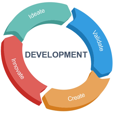
Things are very different now, with all sorts of tools and technologies popping up like mushrooms. For example, I was just chatting with Brad Rex, who is Director, Systems and Solutions, at Renesas. Brad started by noting that today’s traditional development cycles for the “things” (devices) portion of the internet of things (IoT) are cumbersome at best. After researching and defining a new project, engineers have to collect device information and requirements, lay out the hardware, develop the software, and then test and iterate until the product is ready to release to market. This process is typically done sequentially, with each step consuming a significant amount of time. Oftentimes, the software development phase devours the most engineering power and ultimately becomes the biggest bottleneck.
By comparison, Brad says that the future of this class of device development is going to be much faster, nimbler, and more responsive. This includes fast idea generation and the ability to quickly create prototypes for validation, followed by speedy hardware and software development, cumulating in the product launch that is supported by continuous updates.
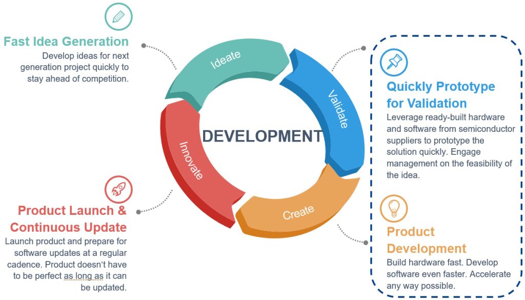
The future of IoT development (Source: Renesas)
Of course, like many things, this sounds wonderful if you speak quickly and gesticulate enthusiastically, but how is this nirvana to be achieved?
Well, as you may recall, last year the guys and gals at Renesas introduced Quick Connect IoT, which provides a collection of standard hardware and software building blocks. The idea is to be able to quickly build a system prototype using standard kits and to generate system projects automatically. Based on standard interfaces like PMOD, Arduino, and MIKROE, this expands beyond Renesas itself to include devices, design houses, system integrators, and cloud vendors (e.g., AWS and Azure).
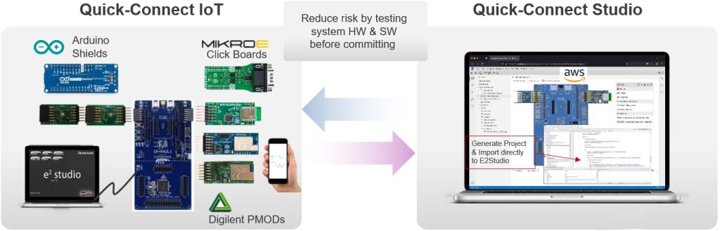
Quick-Connect IoT meets Quick-Connect Studio (Source: Renesas)
Now, the capabilities of Quick-Connect IoT have been enhanced by the addition of Quick-Connect Studio, which is an online, cloud-based design platform that enables users to graphically build hardware and software to quickly validate prototypes and accelerate product development.
With Quick-Connect Studio, engineers can use a browser-based GUI to visually drag and drop device and subsystem blocks in the cloud to build their solution. Even better, the platform automatically generates, compiles, and builds software, thereby taking us one step further towards no-code development. As a result, users can build a full solution in the cloud and quickly deploy that solution to hardware in their lab in less than 10 minutes.
By means of standard connectors, engineers can mix and match MCUs, MPUs, sensors, and connectivity boards (Bluetooth, Wi-Fi) seamlessly. Very little upfront learning or investment is required, the power of cloud compute provides extremely fast compilation, and the modern GUI reduces the learning curve and promotes project reuse.
I can imagine crusty embedded engineers muttering under their breath that this isn’t the way things should be done. “If it’s too easy, then everyone will be doing it,” they will say, but that’s sort of the point. When taken to fruition, this type of technology will enable anyone with a good idea to build a prototype and try it out. If it works, they have a proof-of-concept they can wave around in the hope of persuading someone to fund taking their baby into full production.
What say you? Do you think Quick-Connect Studio heralds the future of IoT development, or do you think a design isn’t worth its salt unless it involves a substantial amount of suffering on the part of its creator?


Back in those days when you told people what you did, did they look at you with raised eyebrows and say “What?”?
That was also about the time that logic designers went from project to project, company to company.
A group assembled to start a new design and one member observed “there are 28 logic designers in the whole world and they just go from project to project”.
Sure enough, there are not enough designers. And because “if” evaluates to true or false that does no mean that programmers are logic designers. Program control flows, Logic data flows and are definitely different.
“Back in those days when you told people what you did, did they look at you with raised eyebrows and say ‘What?’?”
They still do. Outside of my work environment, none of my family or friends understands what I do. Ah, the loneliness of the long distance logic designer…