

Sometimes I cast my mind back longingly to my early days as a design engineer when things were so much simpler than they are now. When I was working on my first ASIC, there was no thought of using functional blocks of intellectual property (IP) from third-party vendors because there were no such things as functional blocks of IP from third-party vendors.
Similarly, we didn’t talk in terms of things like “connectivity fabric” because all we had was wires that connected our logic gates and registers together.
As I’ve mentioned before, we didn’t have any design tools other than pencil and paper. Functional verification involved the other members of the team looking at your schematics and asking pointed questions like, “What is this bit supposed to do?” and “Why on Earth did you implement things this way?” Similarly, timing verification involved us identifying critical paths based on experience and then adding up all of the gate and wire delays by hand.
I find it hard to wrap my brain around the complexity of today’s system-on-chip (SoC) designs, many of which involve hundreds of IP blocks, each of which can contain millions of gates. As one example, I was recently exposed to a multi-billion transistor device intended to perform artificial intelligence (AI) and machine learning (ML) tasks at the edge.
My knee-jerk reaction to this is “How on earth can people conceive and implement devices of this complexity?” Of course, I know that one part of the answer is to employ third-party IP wherever you can, thereby leaving yourself free to focus on your internally developed “secret sauce” IP that will differentiate your product from your competitors’ offerings. Another part of the puzzle is to take full advantage of today’s incredibly powerful and sophisticated electronic design automation (EDA) tools.
Speaking of which, I was just chatting with Prakash Narain, who is the CEO of Real Intent. I have a soft spot for companies like Real Intent. Back in those days of yore we used to call the 1990s, there were lots of smaller EDA companies around, each bringing something special to the party. As the years went by, many of these smaller companies were snapped up by industry behemoths like Cadence, Mentor (which was itself acquired by Siemens), and Synopsys.
And then there are companies like Real Intent, which has awesome technologies, yet has somehow managed to maintain its independence. Part of this is due to the fact that Real Intent’s tools are not intended to supplant those of the other players, but rather to enhance the capabilities of other offerings.
Real Intent was founded in 1998 with an initial focus on formal verification products in the form of assertion-based verification. Although formal technology is still used in Real Intent’s products, the company has evolved to be more focused on its suite of static sign-off tools that accelerate early functional verification and provide advanced sign-off for digital designs.
Real Intent’s static sign-off product capabilities include multi-mode clock domain crossing, multi-scenario reset domain crossing, multi-test mode DFT, multi-policy RTL linting, design initialization, and formal linting.
These products lead the market in terms of performance, capacity, accuracy, and completeness. As a result, more than 50 major semiconductor companies use Real Intent’s tools on a worldwide basis. These include some of the world’s largest companies that are developing SoCs for mobile, networking, telecommunication, display graphics, and myriad other applications.
Before we proceed further, in order to make sense of what is to come, we should perhaps remind ourselves that many of today’s designs are extremely power conscious. One aspect of this is that different functional blocks may be put to sleep (or powered off) when not in use (these blocks may employ special data retention registers to maintain critical data while the bulk of the block snoozes away). Other blocks may be subject to dynamic voltage and/or frequency scaling, which are used to adjust the tradeoff between power and performance on an application and/or task-specific basis.
None of this is as easy as I make it sound (LOL). The IP blocks composing the design may have complex and subtle power-related interdependencies, making the design, verification, and debug of these power-conscious projects even more mind-numbingly complicated.
One way in which designers address this complexity is to employ the Unified Power Format (UPF), which is the popular name for the Institute of Electrical and Electronics Engineers (IEEE) standard for specifying power intent in the power optimization of electronic design automation. The initial IEEE 1801-2009 release of the standard was based on a donation from the Accellera organization, and the current release at the time of this writing is IEEE 1801-2018.
One more point we should perhaps discuss is that we tend to visualize processes, like an SoC design process, as flowing from left to right. The term “Shift-left testing” was first coined by Larry Smith in 2001 with respect to software and system testing in which testing is performed earlier in the life cycle (i.e., moved left on the project timeline). It is the first half of the maxim “Test early and often.” Similarly, in the context of electronic design in general and SoC design in particular, “Shift Left” is understood to refer to using tools and methodologies to detect and address problems as early as possible (earlier than was previously possible) in the development process.
All of which brings us back to my conversation with Prakash, who informed me that a lot of the high-level issues in today’s designs end up being connectivity bugs—that is, problems in the connectivity fabric linking everything together, where some of this fabric may be automatically generated.
We aren’t simply talking about missing connections (although these occur more often than you might expect), but more subtle problems like bits being flipped such that bits 1, 2, and 3 from a source are connected to bits 3, 2, and 1 of a destination, for example. Another potential problem is abutment issues in which connectivity logic is mistakenly inserted between two IP blocks that are intended to be butted up against each other.
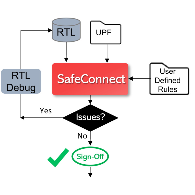
In order to address all this, Real Intent recently introduced their SafeConnect Connectivity & Glitch tool. Like the other members of Real Intent’s suite, SafeConnect is a static analysis tool, which means it doesn’t require a testbench or a simulator. Instead, it analyzes the design’s register transfer level (RTL) design early in the development cycle, allowing designers to quickly identify and resolve any connectivity issues.
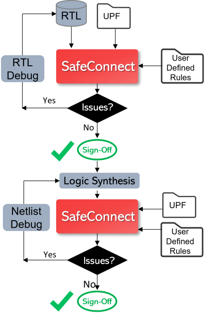
Shift Left with early RTL and netlist sign-off (Source: Real Intent)
In addition to RTL, SafeConnect can also make use of the UPF representation of the design along with a library of user-defined rules. Furthermore, following logic synthesis, SafeConnect can be rerun on the gate-level netlist view of the design.
Many SoC design teams already perform rudimentary connectivity checking by means of Tcl scripts, the creation and maintenance of which can be a nightmare. There’s also the fact that running these sorts of Tcl scripts on a multi-million gate SoC design is a slow and painful process. Furthermore, all a Tcl script can do is tell you that there’s a problem, but it’s of little use when it comes to debugging that problem.
By comparison, Prakash says that SafeConnect features a highly customized and very simple method for developing rules that are tailored to the user’s IP and/or SoC design flows. Once developed, this library of rules is easy to use and maintain. Since SafeConnect employs these rules in a native fashion, it offers the highest speed and capacity in the industry, performing a block-level analysis in a matter of minutes, as compared to hours for Tcl scripting and formal analysis performed on comparable blocks. And, just to add a great big dollop of metaphorical whipped cream on top of our allegorical cake, SafeConnect is fully integrated with Real Intent’s familiar iDebug environment, thereby facilitating the task of tracking each bug back to its lair.
As usual, I’ve only tentatively touched on this topic and barely hinted at the capabilities offered by SafeConnect. If you want to learn more about this and other offerings from Real Intent, why not drop them an email or give them a call and ask them to tell you more (don’t forget to tell them that “Max says ‘Hi!’”).
I only wish I could travel back in time and tell my fellow ASIC designers circa 1980 what the future was destined to hold in the form of SoC design, verification, and debug tools and technologies. How about you? What do you think about all of this?


