


Stuart Pann, Senior Vice President of Intel’s Corporate Planning Group, published an interesting “opinion” piece titled “Expanding Intel’s Foundry Partnerships: A Critical Piece of IDM 2.0” in August. “IDM 2.0” is the term Intel uses to describe its use of process technologies from other foundries in addition to Intel’s home-grown process technologies. The term “IDM” means “integrated device manufacturer” and refers to a chipmaker that manufactures its own silicon die.
In his article, Pann writes:
“I’m asked: Why do we use foundries for products instead of our internal factory network and how do we make that decision?”
He then answers this question:
“Intel has been using external foundries for decades. In fact, Intel currently runs as much as 20 percent of its overall product volume at external foundries, and we are among the top customers of TSMC. Historically we have partnered with foundries to manufacture components such as Wi-Fi modules and chipsets or specific product lines such as Ethernet controllers. These products use mainstream process nodes to complement our internal leading-edge technologies.”
Well that’s part of the answer, so let’s work with that portion first. I think this answer is one that former Intel CEO Bob Swan could and should have given last year when he announced that Intel’s 7nm process (now renamed “Intel 4”) would be delayed by a year and that Intel might be considering other foundries for manufacturing help. At the time, Swan said:
“We will continue to invest in our future process technology roadmap, but we will be pragmatic and objective in deploying the process technology that delivers the most predictability and performance for our customers, whether that be on our process, external foundry process, or a combination of both.”
I think one of the reasons Pat Gelsinger became CEO was because Swan did not publicly convey this reality very well, and it reflected poorly on Intel (and therefore Intel’s stock price). Certainly that’s not the only reason; the one-year 7nm process delay and relative financial performance versus Intel’s competitors are two much bigger reasons, but it’s certainly one of the reasons.
When Intel’s product mix largely consisted of microprocessors, microprocessors, and more microprocessors, the company only needed only one process technology: The fastest, densest technology possible at the time. However, Intel has entered multiple adjacent markets by acquiring diverse chip companies such as Altera (getting power module maker Enpirion in the same deal), Barefoot Networks, Mobileye, and Habana Labs. When it acquires these companies and their products, it also acquires their existing relationships with their chip suppliers.
It makes no sense to migrate these acquired chip designs to Intel internal process nodes. It takes a significant amount of time and resources to redesign a chip for a different technology. These resources are better spent on new products and new product generations.
Stuart Pann’s initial explanation is correct in his August 19 article, but it’s only a partial explanation. There’s another powerful reason for turning to outside foundries, and that reason is based on the way that Intel and other chipmakers are trying to juice Moore’s Law and keep it as alive as possible. That reason is the accelerating push to manufacture multichip modules rather than monolithic ICs. Moore’s Law describes the economic benefits of shrinking process technology to put an exponentially increasing number of transistors on one silicon die.
Single-die Integrated circuits were largely the only way that chips were made for the first 50 years, with some notable exceptions. For example, Mostek produced a 32 Kbit DRAM called the MK4332 in 1979. It combined two MK4116 16 Kbit DRAM diesdie in one multichip package. The MK4332 DRAM’s ceramic package served as the substrate for the two separately packaged MK4116 devices.
Jumping to more modern times, Xilinx announced the Virtex-7 2000T FPGA in 2011. It incorporates four FPGA tiles attached to a silicon interposer to create a large FPGA in a package with nearly 2M logic cells.
Sometimes, placing multiple chips in one package is the only way to achieve the goals for the packaged device. For the Mostek MK4332 DRAM and the Xilinx Virtex-7 2000T FPGA, the goal that could not be achieved without multiple diesdie was the desired capacity. The process technology of the day just wasn’t up to the task. So these earlier multichip devices represented a way of leapfrogging the process technology curve. ThisThe essentially provided a way to juice Moore’s Law.
The Intel Ponte Vecchio GPU, based on Intel’s relatively new Xe graphics architecture, is an extreme example of multichip packaging. The Ponte Vecchio package combines 47 active “tiles” (Intel’s word for “dies”) manufactured with five different semiconductor process nodes from multiple vendors in one package using 3D and 2.5D assembly techniques to produce a product with more than 100 billion transistors.
Certainly, Intel is using multichip packaging to achieve a transistor count not achievable with current monolithic process technology. However, that’s only one reason Ponte Vecchio uses multiple process nodes.
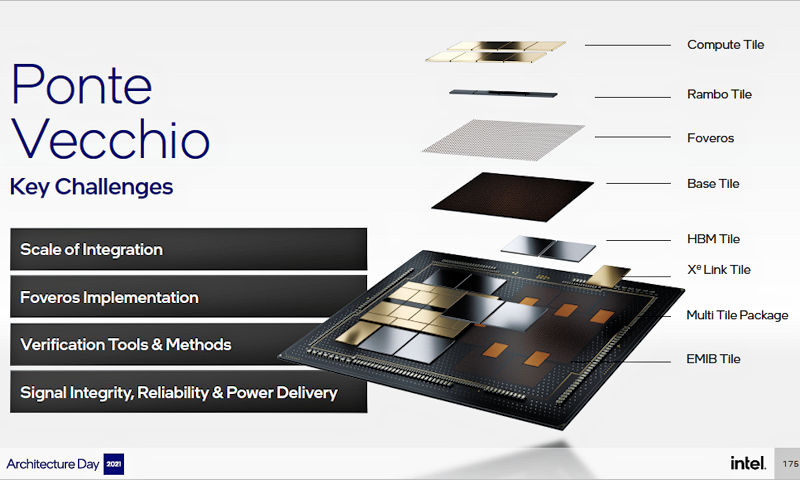
Intel’s Ponte Vecchio GPU combines 47 active “tiles” (dies) manufactured with five different process technologies in one package.
Not all of the process nodes used to make the Ponte Vecchio tiles are Intel process nodes. As Stuart Pann wrote in his opinion piece (the emphasis in bold face is mine):
“As part of Intel’s IDM 2.0 strategy that CEO Pat Gelsinger announced in March, we are evolving this integrated device manufacturer model to deepen and expand our partnerships with leading foundries. These Xe graphics products are part of the first phase of evolution, where we are tapping into another foundry’s advanced nodes for the first time. The reason is simple: Just as our designers use the right architecture for the right workload, we also choose the node that best fits that architecture. At this point in time, these foundry nodes are the right choice for our discrete graphics products.”
He also wrote:
“The next evolution is driven by our modular approach to architecture, which allows us to mix and match individual pieces of silicon – or tiles – on different process nodes and connect them through Intel’s advanced packaging. As more and more semiconductor products transition from systems-on-a-chip to systems-on-a-package technology, Intel’s leadership in advanced packaging will position us to take advantage of this trend. This is already taking shape with Ponte Vecchio, and we are embracing this trend wholeheartedly with upcoming high-volume products such as Meteor Lake for client computing. As we have disclosed, the Meteor Lake compute tile will be manufactured using our leading-edge Intel 4 process technology, with some supporting tiles manufactured at TSMC.”
The real point I’m making here is that chip design today is becoming more like what board design was for the last 50 years with the help of multichip packaging techniques. When designing a circuit board full of chips, we don’t assume that every integrated circuit will come from the same manufacturer. We want to use the “best” chip for each function, based on some multidimensional matrix that allows us to define “best” for each project. You might easily combine an Intel, Qualcomm, or NXP microprocessor or SoC; with a Xilinx or Lattice FPGA; SDRAM from Samsung or Micron,; and Flash memory from Samsung, Kioxia, Micron, or SK Hynix. In fact, you likely do this sort of design routinely. Somehow, it becomes news when an IDM does it.
However, it’s not really news, because all fabless chipmakers already use outside foundries, by definition. It’s not news because chipmakers have been making multichip modules for decades. It’s not news because Intel has been using other foundries for many years.
It is news because this is the first time Intel has announced that it’s using advanced process technology nodes from other foundries, a disclosure that seems to have crossed some sort of mythical line for many Intel observers. But isn’t this a reasonable, logical decision for Intel to make? With Ponte Vecchio, Intel is merely traveling a path that leads directly from the industry’s past and into its future.
Finally, you might ask “What’s next? Will Intel do something crazy like using other, non-x86 CPU architectures?”
News Flash: Intel already does use non-x86 CPUs in its chips.
Intel FPGAs (formerly Altera FPGAs) have incorporated Arm CPU architectures for many years. Intel’s recently unveiled Mount Evans IPU (infrastructure processing unit) on a chip also incorporates Arm CPU cores; and Intel’s Mobileye has used MIPS CPU cores in its products. Finally, SiFive announced that Intel had licensed SiFive’s RISC-V CPU portfolio earlier this year. In its quest to retain its top position as a semiconductor vendor, Intel needs to adopt any technologies, processes, or business practices that allow it to compete.


