

As part of giving courses on digital logic simulation, along with presentations at technical conferences and guest lectures at universities, I’ve been fortunate enough to have at least sampled a tempting taster of many of the countries in Scandinavia and Western Europe, including Denmark, Norway, Sweden, France, Greece, Germany, Italy, the Netherlands, and Switzerland.
Sad to relate, one of the countries on my “bucket list” that I’ve yet to see is Spain, and one of the cities in Spain I’ve long wished to visit is Barcelona. Several of my English friends have holidayed in Barcelona, and I know some Spanish embedded engineers who hail from that fair city. I’ve heard so many tales about the awesome food scene, including evenings spent in tapas bars munching on plate after plate of the most delightful nibbles, that I’m drooling as I pen these words.
The origins of Barcelona are shrouded in mystery. The ruins of an early settlement, including tombs and dwellings, have been found dating to around 5000 BC. Some sources suggest that Barcelona may have been named after the Carthaginian general Hamilcar Barca, who was supposed to have founded the city in the 3rd century BC, but there is little solid evidence for this. What’s known for sure is that the Romans repurposed whatever was already there as a military encampment and colony called Barcino circa 15 BC, which means the city has remained in the same place for over 2,000 years. Today, of course, Barcelona has evolved into a major cultural, economic, and financial center in southwestern Europe, a transport hub (air, sea, road, and rail), as well as the main biotech hub in Spain.
Even though I’ve not, thus far, been fortunate enough to visit Barcelona, this video featuring the song La Rumba de Barcelona by French-Spanish singer Manu Chao makes me feel as though I already know the metropolis.
Quite apart from anything else, Barcelona is home to the Mobile World Congress, an annual trade show that’s billed as being the largest and most influential connectivity event in the world. The most recent MWC, which was held from February 27 to March 2, 2023, attracted 2,400+ exhibitors and 88,500+ attendees from 202 countries and territories.
Speaking of FPGAs (we weren’t, but we are now), I remember when these little scamps first appeared on the scene. Prior to the arrival of FPGAs, circa the early-1980s, I was working with programmable logic devices (PLDs) like programmable read-only memories (PROMs). We used these devices for a wide variety of tasks, including gathering glue logic together, implementing look-up tables, realizing finite state machines (FSMs), and effecting last minute changes to fix anything we’d messed up in the main design.
As I recall, Xilinx announced the first FPGA, the XC2064, in 1984 and delivered it in 1985. The XC2064 boasted an 8 x 8 array of configurable logic block (CLB) “islands,” each containing two 3-input look-up tables (LUTs), all floating in a “sea” of programmable interconnect. Unfortunately, there were no sophisticated design tools for these devices; you were obliged to define the contents of each LUT by hand, and you had to specify how the interconnect was to be configured by hand also.
One of the things we loved about PLDs was their determinism. Their data sheets specified precise input-to-output delays. By comparison, with FPGAs, we didn’t have a clue how they were going to behave delay-wise (now, of course, we specify the timing constraints and leave it to the tools to figure things out).
I remember chatting with some of my engineer friends circa 1985. The consensus was that FPGAs would never catch on. Yes, you are correct, we certainly do feel silly now.
I can’t believe that 1985 is now almost 40 years ago in the rearview mirror of my life. In those days of yore, we never dreamed how FPGAs were destined to evolve, with high-end devices offering logic capacities and performance numbers that make my eyes water just thinking about it.
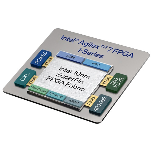
For example, I’m thinking of the Agilex 7 family of FPGAs and SoC FPGAs, which Intel introduced to service the extreme capacity and performance requirements demanded by applications like the network core and data centers. The first members of the Agilex 7 family, the F-Series and I-Series, are built using Intel 10 nm SuperFin process technology. More recently, Intel introduced the Agilex 7 M-Series, which is built using Intel 7 process technology and which expands upon Agilex 7 F-Series and I-Series features by offering in-package high-bandwidth memory (HBM), interfaces for external DDR5 SDRAM, and a hard Network-on-Chip (NoC) to maximize memory bandwidth.
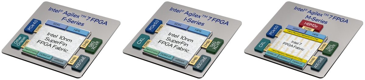
Intel Agilex 7 FPGA and SoC FPGA family members (Source: Intel)
In this context, the difference between FPGAs and SoC FPGAs is that the latter include an Arm Cortex-A53-based 32-bit quad-core hard processor system (HPS) (both types can support multiple soft-core processors implemented in the programmable fabric).
One aspect of these devices that’s really interesting is their use of chiplets, also known as tiles, which are small integrated circuit dice containing a well-defined subset of hardened functionality. In addition to the main FPGA die, Intel Agilex 7 devices can contain between one and six hardened transceiver (XCVR) tiles. These tiles—and the HMB2E stacks in the case of M-Series devices—are connected to the main FPGA die using Intel embedded multi-die interconnect bridge (EMIB) technology. EMIB is an elegant and cost-effective approach to the in-package high density interconnect of heterogeneous chips. The result is that all of these chiplets function as if they are a single large die.
To complement their extreme processing capability, Intel Agilex 7 devices support multiple types of XCVR tiles, including E-Tiles, F-Tiles, P-Tiles, and R-Tiles. Different members of the Intel Agilex FPGA family provide different numbers and combinations of these tiles. Facilitated by Intel’s EMIB and chiplet technology system, integrators have the possibility to devise a broad variety of XCVR capabilities utilizing different tile combinations. This allows customers to employ hardened transceivers while keeping the full capacity and flexibility of the FPGA soft logic. F-Tiles can support up to 400 Gbps Ethernet, while R Tiles can support PCIe 5.0 and CXL interfaces.
The reason for my waffling (yes, this is where I bring everything together) is that a bunch of my chums from Intel attended this year’s MWC just a couple of weeks ago as I pen these words. I can’t tell you everything that Intel showed at the show, if you see what I mean, but the Intel Programmable Solutions Group (PSG) did post this summary highlighting their portion of the proceedings. Of particular interest for me was a whitepaper and two solutions briefs as follows:
- Build Efficient and Cost-Effective mMIMO Solutions with Intel Agilex 7 FPGAs: With respect to radio towers transmitting and receiving wireless signals, this little scamp provides an easy-to-understand introduction to the difference between omnidirectional transmission, MIMO beamforming, and today’s next-generation massive MIMO (mMIMO) technology.
- Intel’s Accelerated Virtual Cell Site Router Solution on an Intel FPGA-Based SmartNIC N6000-PL Platform Helps Communication Service Providers (CoSPs) Increase Monetization of Their Services: Having read this little rascal, I now know the difference between a 4G radio access network (RAN) and a 5G RAN. I’ve also learned what a cell site router (CSR) is and what it does. I’ve also discovered that, as opposed to deploying a CSR as a dedicated box, it’s better to implement it as a virtual CSR (vCSR); also, that Intel has an accelerated vCSR solution in the form of a single Intel Agilex 7 FPGA-based SmartNIC—the Intel FPGA SmartNIC N6000-PL Platform—which can be plugged into an X86 server acting as a virtual distributed unit (vDU).
- Implementing Advanced Networking Solutions with F-Tiles in Intel Agilex 7 FPGAs: “Good Golly Miss Molly,” is all I can say after reading this little ragamuffin. Do you remember the XCVR chiplets we were discussing earlier in the form of E-Tiles, F-Tiles, P-Tiles, and R-Tiles? Well, this paper focuses on F-Tiles deployed in Agilex 7 FPGAs. In particular, it discusses F-Tiles for radio applications (e.g., JESD204 and Ethernet), F-Tiles for fronthaul applications (e.g., gateways, vCSRs), and F-Tiles for passive optical network (PON) applications (I now know what the acronyms OLT, ODN, and ONU stand for, and I have a much better appreciation for the “burstiness” of data as it appears at the OLT).
The more I think about it, the more I realize how lucky I’ve been in so many ways. When I wore a younger man’s clothes, for example, I attended live performances by some of the great artists of the time, like The Police, Supertramp, The Rolling Stones, 10cc, Elton John, Genesis, Led Zeppelin, and Crosby, Stills, and Nash, to name but a few. One act I regret not seeing live was Queen, but I just took a couple of minutes to watch this video of Barcelona, which is the title song of the collaborative album by Freddie Mercury and soprano Montserrat Caballé.
Now I want to visit Barcelona more than ever. I also want to attend MWC 2024. All I need is to find some company that wants to pay me to go. While I’m waiting for the offers to flood in, I’ll start cogitating and ruminating over the Hawaiian shirt wardrobe I’ll need for the trip. In the meantime, as always, I’ll be interested to hear your thoughts pertaining to anything you’ve read here (including tips for the best restaurants to visit and the “must-see” sights to see in Barcelona).


Old PLD/CPLD chip designer here. In addition to the FPGA by-hand-design requirement, I believed that FPGAs had a fatal flaw in that they had to be rebooted from a separate memory like a microprocessor and argued FPGAs would never be accepted by hardware board designers for mass production. Boy was I wrong…
It’s like they say — “Hindsight is the only exact science” LOL
But FPGAs are so expensive! Compared to the cost to build an ASIC?
But FPGAs are so slow! Learn what the fast embedded memory blocks can do for you. And they come in true dual port flavors, yummy. And while you are at it brush up on your microprogramming.
If you still have some spare time, re-visit out of order execution, branch guessing, edge triggered flip-flops versus polarity hold/latches, multi-level caches, clock skew, HLS, use of HDL for design entry…
My take is that so much has been passed on from out dated concepts that it is sickening.
Back to the article … Intel is now pushing NIOS-v (or whatever they call, their soft core contraption) that has separate instruction and data memories. So much for self modifying code and JIT compilation.
The cream on the cake is the worshiping of RISC which is based on the fact that compiler designers could not figure out how to use anything more than load/store/branch/add and subtract.
Let me remind you that the biggest thing limiting cpu performance is memory access time, and let you figure out if using more load and store instructions is a good idea.
The big thing about FPGAs is that they can implement appropriate algorithms in a massively parallel fashion, which lets them race to do things MCUs would do at a crawl. I personally think of soft processors implemented in the programmable fabric more in the form of commend and control as opposed to heavy duty data processing. I think moving to RISC-V (which is what Intel’s NIOS-V is) is a great idea to leverage the existing RISC-V momentum and evolving tools and ecosystem. Re RISC and CISC, I balance precariously on the fence.
It’s interesting how today so many different processor architectures have found their place in the market. While CPUs and ASICs definitely have their place, there are many applications (like the ones in the whitepapers) where they don’t.
You’ve raised valid points about the cost and performance trade-offs between FPGAs and ASICs. Indeed, in high-volume production, ASICs can be more cost-effective, while FPGAs provide flexibility and faster time-to-market for smaller-scale projects or prototypes while providing ASIC-like low latency, high bandwidth performance which with many functions may not be possible to meet spec in using a CPU.
As for NIOS-V and RISC architectures, there are trade-offs to consider based on the requirements of each project. While RISC may simplify instruction sets and improve compiler efficiency, more complex instructions can be beneficial in certain use cases. One of the super cool things about NIOS is the ability to make custom instruction sets which can allow for greater performance in specific applications.
You’re absolutely right that memory access time is a significant bottleneck for CPU performance. Techniques like caching, prefetching, and out-of-order execution can help mitigate this issue.
Let’s see: prefetching dates back to IBM’s Stretch which was a failure. Dr. Fred Brooks said later “It had everything, it even had Gargoyles(he was one of the developers who later was one of the System60 developers.
Out of order execution was a feature of the 360 model 91 which focused on matrix inversion and was not a general purpose computer. Out of order was possible because it had interleaved memory access that allowed 2 outstanding accesses to even and odd addresses — usually one for data and the other for the next instruction.
Then came the mod85 and cache. It was ASSUMED the the hit ratio would be above 90%. That was never quantified because it varied all over the place depending on the application. Also cache to backing store were a cache line at a time which tied up the memory data bus for 8 to 16 double word transfers. Meanwhile everything else waited.\
” Techniques like caching, prefetching, and out-of-order execution can help mitigate this issue.”
Maybe.
Hi, Bret: I would like to add something about FPGAs. They have embedded block rams that have great potential and nobody is looking.
These blocks have dual port mode so two operands can be read for the next execution while the current results are being read. Three memory accesses in parallel!
But these memories are small………….Ya don’t need gigabyte memory on an embedded processor!
#1 there are not hundreds of users running hundreds of applications.
As a point of reference: NASA Houston flew a crew to and from the moon using a cluster of four 360/75 computers each with 1 meg of 8 byte words. (They were 360/75 Model J) And I am asking myself: “Really?” Well they did not have anywhere near the amount of memory on my desktop. And they were programmed in Assembly (C was invented years later).
So what could be done with an FPGA that has all that memory that nobody knows how to use? I am trying to fix that.
” I think moving to RISC-V (which is what Intel’s NIOS-V is) is a great idea to leverage the existing RISC-V momentum and evolving tools and ecosystem. Re RISC and CISC, I balance precariously on the fence.”
Yes it has momentum. It is using antique tools and an academic model (SCALA?) A RISC IS A RISC AND WILL ALWAYS BE A RISC. Load (1 memory access), I fetch (another memory access), maybe another load if the data is not immediate or in a register. And there is not much to do excepts wait for memory.
Ever since von Neumann: load, add, store, brannch ad nausium(spell check?) Ya cain’t really tell one from the other.
Then there was Professor “Complexity is what sells” Dykstra who created the Shunting yard Algorithm. And it won’t work without a stack. There once was a stack, but it disappeared with the Model T (in computer hardware, but not in software). How long has it been since Reverse Polish Notation was invented?
Then to make matters worse, there is a shortage of Cobol programmers and IBM still selling system Z which in my opinion is the CISCiest of the CISC. It does pack, unpack, and decimal divide that Cobol needs.