

If you drive south from downtown San Jose, California on US 101, you’ll soon see a commanding hill rising high above the city’s suburban landscape. A huge monolith commands the crest of this hill. Several large microwave horns once perched upon this tower as if it were a concrete throne. Some remain. The microwave tower was part of the AT&T Long Lines telephone network. The former Xilinx campus, now AMD, is close to this landmark. One of the company’s device families – the Zynq UltraScale+ RFSoC – has figuratively sat alone upon the concrete throne of the semiconductor industry’s own communications hill for the past five years.
Originally announced in early 2017, the AMD/Xilinx RFSoC combined a Zynq UltraScale+ SoC die with on-die 6.544 GSamples/sec RF DACs and 4.096 GSamples/sec RF ADCs to create the world’s first commercial analog-RF-capable programmable-logic device. The Xilinx RFSoC offered real breakthrough technology to RF system designers, and it was unchallenged in the market.
Until now.
Last week at the Intel Innovation event held in downtown San Jose, Intel tossed its RF ante into the pot and took control of programmable logic’s RF poker game by announcing an analog-enabled portfolio of FPGAs and other logic devices that incorporate RF ADCs and DACs capable of achieving 64 GSamples/sec, per converter. The capabilities of the devices in this analog-enabled product portfolio redefines what’s possible with direct-RF conversion at frequencies that were previously far beyond reach.
RF design was almost entirely analog before high-speed data converters and DSPs were developed. RF signal processing involved the use of filters and mixers drawn from the rich, decades-long heritage of tube-based superheterodyne radio receivers first developed by Edwin Armstrong during World War I. These circuits down-converted RF signals into baseband frequencies to prepare them for DSP at the lower processing rates that could be achieved by the hardware of the day.
The advent of ADCs and DACs that operate at tens of GSamples/sec makes it possible to develop direct-RF architectures that eliminate most of the expensive analog filters and mixers employed in superheterodyne RF designs. Direct-RF conversion techniques increase system performance, decrease system-level costs, and reduce SWAP (size, weight, and power). Although there are many applications including data center networking, optical transport, 8K video, and 5G wireless that might use this technology, it’s most likely that the devices in this new analog-enabled programmable-logic portfolio will initially make its way into military/aerospace equipment such as radar, SIGINT (signal intelligence), and EW (electronic warfare) systems.
In fact, Intel announced early last year that this technology had been developed under the US DARPA CHIPS (Common Heterogeneous Integration and Intellectual Property (IP) Reuse Strategies) program (not to be confused with the recent US CHIPS Act) in partnership with Lockheed Martin and BAE Systems. Both companies are military contractors. Here’s a quote from the Lockheed Martin Web site, attributed to Deon Viergutz, vice president of Lockheed Martin’s Spectrum Convergence organization:
“This technology allows us to integrate our latest generation electronic warfare systems into smaller airborne platforms and air launched effects that were previously unattainable due to size constraints of the air vehicle. As a result, we’ve created the Ultra Small Affordable Electronic Warfare (USAEW) sensor that provides the 21st century warfighter advanced capabilities while substantially reducing the systems’ size, weight, power and cost by an order of magnitude.”
These days, digital RF applications generally rely on JESD204 high-speed serial protocols to interface RF DACs and ADCs to digital processing circuitry. The JESD204 interface replaced earlier, parallel, device-to-device interfaces, which were growing overly power hungry as conversion rates climbed into the GSamples/sec domain. PCB routing of the many high-speed parallel connections was also getting difficult. However, the JESD204 protocols inserted the latency of a serial connection and, eventually, even JESD204 connections started to require high I/O power consumption to drive multiple PCB traces at multi-Gbps data rates.
Many military/aerospace applications cannot tolerate the latency overhead imposed by the JESD204 interface protocol. These kinds of real-time RF applications require a different sort of high-speed analog converter interface that consumes less power and exhibits much lower latency. As shown below, devices in the new analog-enabled Intel FPGA portfolio connect FPGA die with RF DAC and ADC chiplets using Intel’s EMIB and AIB die-to-die interconnect technologies, which require less interface power and deliver much lower latency because they’re based on massively parallel connectivity and very short, die-to-die connections with very low impedance.
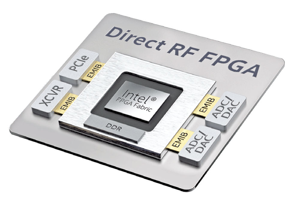
Image credit: Intel
EMIB is a practical and now long-proven die-to-die interconnect technology that’s relatively easy for chip designers to implement. Intel has used the EMIB and AIB interconnect technologies to build Stratix 10 and Agilex FPGAs and SoCs for several years, so it’s quite logical (pun intended) for the company to use these technologies to attach RF DACs and ADCs to its programmable-logic silicon to create an analog-enabled FPGA and SoC portfolio. EMIB greatly resembles high-density PCB wiring but at a much smaller scale that is aimed at the device package level, with trace-to-trace and pad spacing appropriate for chip-scale packaging. AIB is a very wide, multi-channel, high-speed, low-power parallel bus with a simple clocked interface bus protocol designed specifically to meet the requirements for die-to-die interconnect.
It would be even more efficient to integrate the RF DACs and ADCs directly into a monolithic programmable-logic device, but these RF circuits are excellent examples of functions that should not and could not be built using the same semiconductor processes used to fabricate FPGAs. RF converters require a different semiconductor process technology, not one tuned for high-speed digital logic. Intel’s analog-enabled portfolio is therefore a validation of the heterogeneous, chiplet-based construction approach now being adopted across the semiconductor industry.
However, Intel says its analog-enabled FPGA portfolio is not limited to using programmable-logic die. The company also offers eASIC structured ASICs and will build full-custom ASICs for the right customers. All of these logic die can be connected to RF DACs and ADCs using EMIB and AIB. It’s a natural extension of the technology, and the announcement of Intel Foundry Services in March of 2021 underscored Intel’s renewed and very public interest in using this kind of technology to develop custom devices for the right customers.
In addition, Intel is not limiting the devices in the analog-enabled device portfolio to the 64-GSamples/sec analog converters. The company plans to offer other devices in the portfolio equipped with somewhat slower RF DACs and ADCs, according to customer requirements. The company envisions that its growing chiplet library might be used to quickly construct many types of devices. That chiplet library currently includes the various FPGA fabric die; digital interconnect chiplets including 58G and 116G SerDes transceivers used to implement 50/100/200G Ethernet and PCIe 4.0/5.0 connections, coherent CXL connections among CPUs, and more specialized chiplets that implement specific capabilities such as DSP and networking.
The extended chiplet library also includes HBM (high-bandwidth memory) stacks made by other semiconductor vendors and five chiplets from Defense Industrial Base suppliers. These Defense Industrial Base chiplets are a direct result of the DARPA CHIPS program. Intel released AIB as a royalty-free chiplet interconnect standard to DARPA’s CHIPS program in 2018 and the CHIPS Alliance (a Linux Foundation project not to be confused with the US CHIPS Act or the DARPA CHIPS program) subsequently published the AIB specification as a royalty-free standard.
The AMD/Xilinx University Program has had tremendous success with an RF engineering education kit based on its first- and second-generation RFSoCs. These kits are being used to develop state-of-the-art communications and instrumentation applications in application areas as diverse as software-defined radio (SDR), radar, radio astronomy, quantum computing, spectroscopy, and AI/ML for SDR.
One reason for the success of the AMD/Xilinx RFSoC is because the RFSoC-PYNQ framework, based on the company’s PYNQ project, uses Jupyter Notebooks and the JupyterLab integrated development environment (IDE) that data scientists have been using for years. The RFSoC-PYNQ framework makes RF development more accessible to a much wider range of scientists, engineers, and software developers.
AMD/Xilinx now offers RFSoCs with faster RF ADCs and DACs, up to 5.9 and 9.851 GSamples/sec respectively, but Intel has clearly leapfrogged its competitor with the new analog-enabled FPGA portfolio. Although Intel’s announcement didn’t mention any RF-specific development tools for the analog-enabled FPGA portfolio, Intel is vying for the right to become king of the industry’s Communications Hill, so perhaps such tools are not too far in the future. Vive le competition.


Correction. You mention that Xilinx’s Zynq RFSoC consists of an RF Die and FPGA Die in a 2.5D package, when in fact the Zynq RFSoC devices are monolithic dies with both the RF and FPGA logic sitting together on that die. This provides an impressive low power, potentially low cost, solution.
The Intel Chiplet approach is certainly impressive at 64GS/s but I suspect that the two devices will co-exist and serve different markets more than they compete.
All that being said this is excellent progress from Intel with everything that can be potentially achieved with Direct Digital RF albeit with a relatively power hungry solution.
Hi,
After looking at X-Ray images of the Zynq RF SoC (from post PCB assembly inspection), I am fairly sure that the RF data converter tiles are on separate dies from the FPGA die. They appear to be mounted on an interposer with a fine pitch ball grid array, not dissimilar to what Intel are now looking at with their chiplet approach maybe?
Regards
Mike
As a further note, the part I am talking about is a ZU28DR gen 1 device and so Xilinx may well have integrated all onto a single die in the more recent Gen3 devices such as ZU48DR , thanks
I also thought this way, @slipstream_mike, but I checked the original 2017 press release for the RFSoC. It specifically says “monolithic.” I believed the original RFSOC had multiple die, but my memory seems to have been in error. I just took this from the AMD RFSoC page:
“The monolithic integration of direct RF-sampling data converters onto an adaptive SoC eliminates the need for external data converters, enabling a flexible solution with up to 50% reduced power and footprint over a multi-component solution–including the elimination of the power-hungry FPGA-to-Analog interfaces like JESD204. This approach also enables a highly flexible solution, moving much of the RF signal processing into the digital domain.”
If that’s not currently accurate, then you have a beef with AMD.
You are correct acantle1. I stand corrected and have updated the article accordingly. Thanks for the correction! I agree with you that both devices are likely to succeed in the marketplace. I was trying to indicate that with my discussion of the AMD/Xilinx software tools. Perhaps I should have been more explicit.
Interestingly the new D series AgileX (also just announced) which targets smaller device sizes moved away from multi-die EMIB and a number of previously available EMIB interface die are now part of the monolithic die in the D-Series. There is no RF option listed in the product table and the max size is 1/2 that of Arria10 family at TSMC. Perhaps one or both capabilities are being held in reserve?
Fully agree the 64G product is in itself very intriguing, due to the impressive order of magnitude improvement in ADC/DAC sample rates available in an FPGA making accessible a whole range of market space to date only addressable with ASICs. Will be interesting to see what is possible with this RF device.
@mj_remote I covered the Agilex D-series parts last week in EEJournal. Intel’s analog-enabled FPGAs all reserve the RF analog I/O for 3rd-party chiplets. That means Intel likely does not have high-speed DAC IP in house nor would 3rd-party RF analog IP be compatible with the Intel 7 digital CMOS process. Also, the new monolithic Agilex families do not currently have AIB ports (no need since they’re not EMIB devices). So the chances are slim that Intel is holding analog RF in reserve for the new Agilex families. It’s not that Intel could not do this, but Intel does not appear to be looking to cost-reduce this world-beating product, for now.