


Last September, I published an article on EEJournal.com that described two new Intel Agilex FPGA and SoC device families, the Agilex 5 D-series and an as-yet-unnamed series formerly known as “Sundance Mesa,” introduced at last year’s Intel Innovation. (See “Intel Introduces Two Monolithic Agilex FPGA and SoC Families, Part 1.”) As discussed in that previous article, the two new FPGA/SoC families share many characteristics starting with their monolithic construction. I expected to follow that first article with a second one describing the Sundance Mesa FPGAs in a couple of days. However, Intel was not yet ready for such a disclosure back in September. Now, it is ready. Intel formally announced that Sundance Mesa is the Intel Agilex 5 E-Series on January 10. In the intervening months, about all that’s changed is the product naming. The Intel Agilex D-Series has become the Intel Agilex 5 D-Series and Sundance Mesa is the Intel Agilex 5 E-Series. Today’s article discusses the differences between these two series of devices, so that you’ll be better able to choose between them for your next FPGA design project.
Perhaps the biggest differences between the Agilex 5 D-Series and E-Series device families are power consumption and package size. Intel Agilex 5 E-Series FPGAs and SoCs come in two flavors: Power-Optimized and Performance-Optimized. Intel Agilex 5 D-series devices come in only one flavor, which is akin to the Agilex 5 E-Series Performance-Optimized form in that it’s optimized for performance. The Power-Optimized Agilex 5 E-Series devices and the Agilex 5 D-series FPGAs and SoCs are SmartVID devices, so they require an external PMBus voltage regulator to run the device at its optimum core voltage, as determined by a factory-set power/performance optimum. You must drive the VCC and VCCP core voltage supplies for these devices with a dedicated PMBus voltage regulator. In exchange, these devices will remain at this power/performance setpoint over their operating temperature range.
Power-Optimized Agilex 5 E-Series FPGAs and SoCs require fixed core power supply voltages of 0.75 and 0.8 V. Device performance is better with the 0.8 V core voltage, but power consumption is lower with the 0.75 V core voltage. The devices’ performance will be somewhat lower at the lower core voltage. Intel explained that these power-optimized devices have lower static power consumption than the SmartVID flavored Agilex 5 E-Series versions. You can use a simplified power supply with these devices, which can reduce system-level costs if you don’t need to wring the maximum speed from the family.
Package size is another significant difference between Agilex 5 D-series and E-Series devices. Both D-series and E-Series device families are available in the unfortunately named “balls anywhere” package design, which has different-sized pads and a mixed ball pitch compared with standard ball grid array (BGA) packages, which have consistent solder ball sizes, pads, and pad pitch, as shown below.
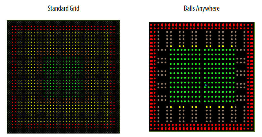
Standard Ball Grid versus “Balls Anywhere” packaging for the Intel Agilex 5 FPGAs and SoCs. Image credit: Intel
Intel says that the “balls anywhere” packaging results in smaller device packages and reduces the number of required circuit board layers. Agilex 5 D-series FPGAs and SoCs are offered only in “balls anywhere” packaging, while Agilex 5 E-Series FPGAs and SoCs are also available with a standard BGA package with the ball pitch set on a 0.5mm grid. Intel says that this BGA format still allows for small packages but with more I/O pins than is possible with the “balls anywhere” packaging, at the cost of possibly requiring more circuit-board layers. If board real estate, overall board size, and circuit board cost are critical for your design, you may well decide to use the “balls anywhere” package. If you need more I/O pins, then you’ll likely favor the conventional BGA package.
More subtle differences between the Agilex 5 D-series and 5 E-Series devices appear in the number of logic elements and block SRAMs in the devices offered within these new families, the number of high-speed SerDes ports supported by each device, the speed of these high-speed SerDes ports, the clock rates for the Hard Processor System (HPS), and the types of DDR SDRAM supported. Each of the new device families incorporates different amounts of on-chip resources, with the Agilex 5 D-series devices going especially heavy with the on-chip SRAM compared to the Agilex 5 E-Series devices.
The Power-Optimized Agilex 5 E-Series device family incorporates 50K to 656K logic elements (LEs) and 130 to 1611 M20K block SRAMs. The Performance-Optimized Agilex 5 E-Series devices incorporate 138K to 656K LEs and 358 to 1611 M20K block SRAMs. Agilex 5 D-series devices incorporate 103 to 644 LEs and 534 to 3204 M20K block SRAMs.
Agilex 5 D-series and Agilex 5 E-Series Performance-Optimized FPGAs and SoCs both incorporate SerDes transceivers that support 28.1 Gbps NRZ data rates. Agilex 5 E-Series Performance-Optimized devices have as many as 24 of these 28.1 Gbps transceivers, while Agilex 5 D-Series devices have as many as 32 of them. Agilex 5 E-Series Power-Optimized devices derate these transceivers to a maximum data rate of 17.16 Gbps and have as many as 24 such transceiver ports.
The three Intel Agilex 5 families also differ in the amount of PCIe support because of these transceiver speed and quantity differences. Agilex 5 D-series devices support PCIe 4.0 x8 operation with as many as four hard PCIe IP controller blocks. Performance-Optimized Agilex 5 E-Series devices have fewer high-speed SerDes ports and therefore can support PCIe 4.0 x4 operation with as many as six hard PCIe IP controller blocks. Power-Optimized Agilex 5 E-Series FPGAs and SoCs do not support PCIe 4.0 at all. Instead, these devices support PCIe 3.0 x4 operation with as many as six hard PCIe IP controller blocks. If a specific PCIe requirement is high on your project’s needs or wants list, these differences alone may clarify your choice.
Similarly, there are some differences in the maximum clock rates for the processors in the HPS blocks incorporated into the Agilex 5 D-series and Agilex 5 E-Series SoC families. For Agilex 5 D-Series and Performance-Optimized Agilex 5 E-Series SoCs, the dual-core Arm Cortex-A76 processor in the HPS runs at a maximum clock rate of 1.8 GHz and the dual-core Arm cortex-A55 processor runs at a maximum clock rate of 1.5 GHz. For Power-Optimized Agilex 5 E-Series SoCs, the dual-core Arm Cortex-A76 processor in the HPS runs at a maximum clock rate of 1.6 GHz and the dual-core Arm cortex-A55 processor runs at a maximum clock rate of 1.33 GHz.
Practically speaking, the 11 percent difference in the Power-Optimized Agilex 5 E-Series SoCs isn’t going to make a lot of overall performance difference. After all, these are FPGAs we’re talking about. System designers are more likely to be using the on-chip programmable logic for the heavy lifting when it comes to executing high-speed tasks. Nevertheless, there could be an advantage to the faster HPS clock rates in some applications, so be aware of the differences.
All new Agilex 5 D-series and Agilex 5 E-Series FPGAs and SoCs contain integrated, hard SDRAM controllers, but the kinds of SDRAM supported by these devices varies in a somewhat complex manner. Agilex 5 D-series devices support:
- DDR5-4000 (2000 MHz, 4000 MTransfers/sec)
- LPDDR5 (2233 MHz, 4267 MTransfers/sec)
- DDR4-3200 (1600 MHz, 3200 MTransfers/sec)
- LPDDR4 (2133 MHz, 4267 MTransfers/sec)
Power-Optimized Agilex 5 E-Series devices support:
- LPDDR5 1200 MHz (2400 MTransfers/sec)
- DDR4-2400 (1200 MHz, 2400 MTransfers/sec)
- LPDDR4 (1333 MHz, 2666 MTransfers/sec)
Performance-Optimized Agilex 5 E-Series devices support:
- DDR5-3600 (1800 MHz, 3600 MTransfers/sec)
- LPDDR5 (1867 MHz, 3733 MTransfers/sec)
- DDR4-3200 (1600 MHz, 3200 MTransfers/sec)
- LPDDR4 (1867 MHz, 3733 MTransfers/sec)
In addition, the Agilex 5 D-series and Performance-Optimized Agilex 5 E-Series devices incorporate hard IP that supports the MIPI D-PHY v2.5 Camera Serial Interface (CSI-2) and Display Serial Interface (DSI) protocols at 3.5 Gbps per lane. The Power-Optimized Agilex 5 E-Series devices also incorporate MIPI D-PHY v2.5 IP but support the protocol at 2.5 Gbps per lane.
Although Intel doesn’t care to use these words, the Agilex 5 D-series and Agilex 5 E-Series devices bolster the company’s position in mid-range and low-end FPGAs. When the company does make comparisons, it compares the Agilex 5 D-series devices to the Stratix 10 family, which is a mid-range family now that the original Agilex family has been on the scene for a few years. The company compares Agilex 5 E-Series devices to its aging Cyclone V family, which are 28nm devices introduced a decade ago. By now, these Cyclone devices are clearly low-end FPGAs and SoCs.
However, the specifications say that these two new Agilex families are anything but low-end FPGAs and SoCs. With their Agilex architectural heritage, many improvements to the HPS, the new Tensor block, and other on-chip resources, cost-reducing monolithic construction, and smaller package sizes, these new Agilex 5 device families deliver some impressive capabilities that are sure to be welcomed by developers of FPGA-based equipment. Meanwhile, Intel is clearly looking to extend the successful Agilex brand even further down the product line spectrum with the newly revealed “power- and cost-optimized” Agilex 3 family of devices in compact form factors. However, Intel is still teasing customers and prospects with the dance of the seven veils when it comes to the Agilex 3 series FPGAs. We’re not allowed to see the details yet. Instead, Intel says that details are “forthcoming.” No doubt, the company will reveal those details in its own sweet time.


Looks like a BIG problem for Lattice’s Avant.
And not just Intel, there are others.