


Intel has just introduced the Agilex M-Series FPGAs with support for PCIe Gen5, Optane persistent memory, CXL, and high-speed Ethernet. Some of the FPGAs in the Agilex M-Series also incorporate integrated High Bandwidth Memory (HBM) DRAM stacks. FPGAs with integrated HBM DRAM stacks are not new. Both Intel and AMD-Xilinx have offered such devices for a few years. Xilinx announced its first FPGAs with integrated HBM, the Virtex UltraScale+ HBM FPGAs, in late 2016, although parts didn’t appear until early 2018. Intel’s first-generation FPGA family with integrated HBM2 DRAM stacks were the Intel Stratix 10 MX FPGAs, announced in late 2018. The Agilex M-Series FPGAs incorporate the latest, fastest, 3rd-generation HBM2e DRAM stacks. These are the same in-package DRAM stacks being used to boost performance in the Fourth Generation Intel Xeon Scalable “Sapphire Rapids” CPUs and the Intel Ponte Vecchio GPU.
There’s one overriding reason to add HBM to an FPGA: speed. Of course, the fastest memory you can get on an FPGA continues to be the local SRAM embedded in the programmable-logic fabric. This sort of memory generally operates as fast as the surrounding logic in the FPGA’s fabric. However, local SRAM resources have limited capacity. FPGA vendors try to create the “best” possible balance of on-chip FPGA resources including logic, memory, and DSP blocks, but of course the optimal resource balance depends on the application, doesn’t it? So, there’s really no such thing as an optimal balance for a general-purpose device like an FPGA.
SRAM blocks consume a considerable amount of memory and externally interfaced DDR SDRAMs are significantly slower, so FPGA manufacturers look for an intermediate memory technology to toss into the FPGA’s memory hierarchy. Intel and Xilinx chose HBM. Adding HBM DRAM stacks to FPGAs is not a cheap choice, which is why you see FPGAs with HBM sitting at apex of each FPGA generation’s performance pyramid. They’re the fastest devices in each generation, so they’re expensive. But they’re fast. Applications that require this sort of memory speed include cloud acceleration, 400GbE and 800GbE networking, next-generation network firewalls, 8K (and higher) broadcast video equipment, military and aerospace phased-array radars, and even high-speed test and measurement gear. These are the sort of applications where the FPGA cost is secondary. Speed is king.
When compared with the HBM2 memory used in Intel Stratix 10 MX FPGAs, the Intel Agilex M-Series FPGAs’ maximum of two in-package HBM2e DRAM stacks double the available high-speed DRAM capacity to a maximum of 32 Gbytes. Each HBM2e DRAM stack also increases memory bandwidth to 410 Gbytes/second, for a total HBM2e memory bandwidth of 820 Gbytes/second. That’s a 60% bandwidth increase compared to the HBM2 memory used in the Intel Stratix 10 MX FPGAs. This additional memory bandwidth opens Agilex M-Series FPGAs to more challenging system designs.
For many system designs, 32 Gbytes of memory capacity will not suffice, so Agilex M-Series FPGAs also supports external DDR5 and LPDDR5 SDRAMs through hardened memory controllers. DDR5 and LPDDR5 SDRAMs are currently the fastest mainstream SDRAM DIMMs available. The Agilex M-Series memory controllers also support QDR-IV SRAMs.
The Agilex M-Series FPGAs also support Intel’s non-volatile Optane persistent memory, which is slower than SDRAM but offers greater capacity. Optane non-volatile memory slips yet another layer into the available memory hierarchy for these FPGAs, which gives you more design flexibility. You may not elect to use this additional flexibility, but it’s there if you happen to need a large amount of relatively fast, non-volatile storage.
The memory controllers in the Intel Agilex M-Series FPGAs can operate DDR5 SDRAM at 5600 MTransfers/second with a data width as wide as 80 bits per channel. According to Intel, if you combine the in-package HBM2e DRAM and external DDR5 SDRAM memory bandwidths, you’ll get a theoretical maximum DRAM memory bandwidth of 1.099 TBytes/second, assuming that eight DDR5 SDRAM DIMMs are attached to the FPGA. That’s a lot of memory bandwidth, and that number does not include the memory bandwidth contribution of the logic fabric’s internal SRAM.
Routing more than a TByte/second of data between the FPGA’s programmable-logic fabric and the HBM2e and DDR5 memories poses quite a challenge for even the most experienced FPGA development team, so the Intel FPGA design team developed a dual, hardened Network on Chip (NoC) for the Agilex M-Series FPGAs, which are the first Intel FPGAs to incorporate a hard NoC. If you peruse the diagram below, the Agilex M-Series NoC is clearly not a general-purpose NoC like the ones you’ll find on Xilinx Versal devices or the Achronix Speedster 7t FPGA, which can connect various on-chip computing elements to each other, to the I/O ports, and to internal and external memory. The Agilex M-Series NoC is designed to transport data between the FPGAs’ memories, its I/O ports, and specifically to the M20K SRAM blocks in the programmable-logic fabric, but not between computing elements in the logic fabric.
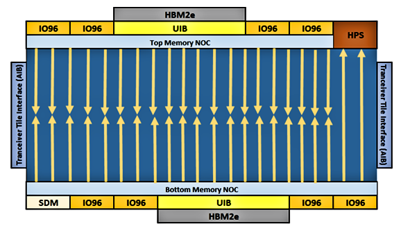
The Intel Agilex M-Series FPGAs have a split NoC that surrounds the programmable-logic fabric and provides high-speed communications between the HBM2e DRAM and DDR5 SDRAMs and the M20K SRAM blocks in the FPGA’s programmable-logic fabric.
If you study the above diagram, you’ll see that the Agilex M-Series NoC is divided into a Top and Bottom Memory NoC. The Top and Bottom Memory NoC components each extend twenty hardened, 256-bit vertical network segments into the programmable-logic fabric to transfer read data from NoC-attached HBM2e and DDR SDRAM memories to (but not from) the M20K SRAM blocks in the fabric. Each of these vertical segments has a peak bandwidth of 22.4 GBytes/second. Keep in mind that these segments convey that traffic outside of the programmable-logic fabric’s normal routing paths, which should significantly reduce routing congestion for memory-related traffic.
Each vertical network segment extends halfway into the logic fabric, either from the Top or Bottom Memory NoC. These vertical NoC segments connect to the M20K blocks embedded in the FPGA’s programmable logic fabric, and they only convey data one way, from the HBM2e and DDR memories to the M20K blocks. Data written to the HBM2e and DDR memories from the fabric and the read/write control logic implemented in the fabric must go to the HBM2e and DDR memories through the logic fabric.
A detailed graphic showing the details of Memory NoCs appears below.
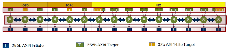
Detail of a section of one half of the Intel Agilex M-Series NoC showing the hardened network switches (green circles), the AXI4 Initiators and Targets, and the AXI4-Lite Targets for writing data to memories and for read/write memory control.
This NoC detail shows that the Top and Bottom Memory NoCs connect to the logic fabric through 256-bit AXI4 Initiators and to the HBM2e DRAM (through the block marked UIB) and to DDR SDRAM and I/O ports (through the IO96 blocks) through 256-bit AXI4 Targets in the NoC. The NoC routes data from source to destination through network switches (shown above as green circles marked with an “S”) and interconnect links. Every AXI4 Initiator can talk to every AXI4 Target in the NoC through full crossbars in the NoC.
The NoC acts like a superhighway in the FPGA and it consumes none of the FPGAs’ internal programmable logic. The Agilex M-Series dual NoCs have an aggregate peak bandwidth of 7.52 Tbps, which greatly reduces the potential for memory bottlenecks.
FPGAs targeting high-end applications like these Intel Agilex M-Series devices must include high-speed SerDes transceivers and the M-Series FPGAs incorporate as many as 72 high-speed transceivers, including as many as eight transceivers that operate at 116 Gbps using PAM4 modulation. These SerDes transceivers support a variety of the newest high-speed serial protocols including 400G Ethernet and can be directly interfaced to the latest CPUs using the PCIe Gen5 and CXL interface protocols.
Considering that we’re discussing FPGAs here, this article has been a bit light on a discussion of the computing capabilities of the Agilex M-Series programmable logic fabric. Because these FPGAs are manufactured using the Intel 7 process node, the programmable-logic fabric in the Intel Agilex M-Series FPGAs should be fast, but Intel only claims that the logic fabric in these FPGAs delivers “over 2X fabric performance per watt vs 7 nm competition,” so we don’t get a good idea of the logic fabric’s maximum speed. That’s typical in FPGA World. The speed you get really depends on your application, your design, and what you can coax out of the development tools. However, Intel has tossed in as many as 12,300 variable-precision, floating-point DSP blocks, capable of delivering 18.5 single-precision TFLOPS or 88.6 INT8 TOPS, into its Agilex M-Series FPGAs, so there’s ample potential for throwing lots of TOPS and TFLOPS at heavy computational loads.
The obvious comparison to the Agilex M-Series FPGAs in the AMD-Xilinx camp is the Versal HBM ACAP, which TSMC fabricates with its 7nm process technology. (I am not about to get into a discussion of whether TSMC’s 7nm or the Intel 7 process technology is más macho in this article.) Like the Agilex M-Series FPGAs, Versal HBM ACAPs also add HBM2e DRAM stacks as another layer in the memory hierarchy. Intel’s announcement lists two devices in the Intel Agilex M-Series while AMD-Xilinx lists five devices in the Versal HBM Series. In comparison to the largest Agilex M-Series FPGA’s 12,300 variable-precision, floating-point DSP blocks, the largest Versal HBM ACAP incorporates 10,848 DSP Engines, which are DSP58 blocks – supersets of the more familiar DSP48E2 DSP block.
Without far more data for both device families, detailed comparisons between the Intel and AMD-Xilinx offerings beyond the high-level comparisons I’ve made in this article are problematic. To my experienced eyes – I’ve written about Intel-Altera and AMD-Xilinx programmable-logic devices for a couple of decades and have worked at both companies – the Intel Agilex M-Series devices look a lot more like traditional, familiar FPGAs and ACAPs – well ACAPs are something very different as the AMD-Xilinx ACAP designation implies. The potential capabilities of the AMD-Xilinx ACAP concept are just now being explored through rapidly evolving development tools specifically tailored for the ACAP universe.
However, it’s quite clear to me that if your next design has enormous memory-bandwidth requirements that go far beyond the norm for programmable logic, both the Intel Agilex M-series FPGAs and AMD-Xilinx Versal ACAPs should be on your short list for consideration. The other FPGA you might consider is the Achronix Speedster7t. It too is manufactured by TSMC using its 7nm process technology and it has a truly interesting, on-chip, 2D NoC developed by Achronix. It also has 112 Gbps SerDes transceivers and a PCIe Gen5 controller, so it’s in the same high-end class of programmable logic device.
Although the Speedster7t FPGA does not incorporate HBM like the offerings from Intel and AMD-Xilinx, its eight built-in memory controllers work with GDDR6 SDRAM, which is considerably faster than DDR5 SDRAM. Achronix claims that the Speedster7t ekes out half a TByte/second of memory bandwidth when all eight DRAM controllers are maxed out on GDDR6 SDRAM. Although that’s only half of the memory bandwidth achieved by the Agilex M-Series FPGAs with HBM, the Achronix Speedster7t FPGA might still offer enough memory bandwidth for your application’s needs. Isn’t it great to have choices up there at the apex of the FPGA pyramid?


Register/Memory transfers are not typical limits for fmax. It is usually the long path for control logic. So this looks like smoke and mirrors to side step the real performance limits.
HDLs, FSMs, and dFFs are far from ideal for design(I would say “useless”) but the only thing that synthesis can cope with.
So Intel is side-stepping the real issue. Logic design is fundamental(but ignored). And having to use spreadsheets to tie logic modules together is ridiculous
And moving data from memory to memory without having the performance to process the data is being ignored. (just as Intel rode the multi-core nonsense into the ground).