


Two presentations during the same week from Intel and Movellus highlighted radically different approaches to solving voltage droop, a problem that increasingly plagues SoC designs as device geometries continue marching down the Moore’s Law curve. Intel, being a manufacturing-centric company, has developed a backside power distribution network (PDN) for its Intel 20A and 18A process nodes. Meanwhile, IP vendor Movellus has developed an extension to its digital, synthesizable clock-network IP, which allows a chip manufactured using any semiconductor process node from any foundry to sense power droop and automatically tune the on-chip clock network to eke maximum performance from the SoC’s limited power envelope.
Voltage droop arises from the IR (current-resistance) losses in a chip’s PDN. Since the first days of ICs, PDNs have been formed in the same metal layers used for routing signals to the chip’s transistors. PDN resistance increased as IC manufacturing evolved from one layer of metal to two, to a dozen, to fifteen or more, with finer and finer line widths at each step along the way. The IR drop became especially noticeable as core voltages dropped from 5 volts to 1 volt, or less. At the same time, transistor power consumption has increased as clock frequencies have risen from megahertz to gigahertz. In addition, today’s SoCs simply incorporate a lot more transistors – “billions and billions” as Carl Sagan might say – that need power. All these factors are responsible for increasing the problems associated with IR droop, which can force an IC to operate at lower-than-maximum frequencies, resulting in sub-optimum performance.
Intel’s approach sounds simple, superficially: just add a dedicated PDN to the back side of the semiconductor die. Small through-silicon vias (“nano TSVs”) carry power from the backside PDN up to the transistor layer buried deep within the chip. The backside PDN moves the PDN from the chip’s top metal layers and delivers power through larger metal layers on the bottom of the chip, which delivers many significant physical design benefits including reduced IR droop, smaller standard-cell footprints, and simplified signal routing on the chip’s top metal layers. Intel calls this approach “PowerVia,” which is akin to adding power and ground planes to a 2-sided circuit board to improve board-level IR drop and noise – a technology that’s been around since the 1970s. However, the modifications to the semiconductor process are not simple from a practical perspective.
Moving the PDN Down Under
Figure 1 below shows the difference between today’s approach (on the left), which integrates the PDN into the top metal-layer stack, and the backside PowerVia PDN as developed by Intel (on the right). As the figure shows, the backside PDN uses larger, thicker metal layers to supply power to the chip’s transistors, which lower PDN resistance and leaves more room for signal routing on the top metal layers. The PowerVia technology requires the addition of wafer-thinning and polishing process steps in addition to the need to perforate the wafer with nano TSVs.
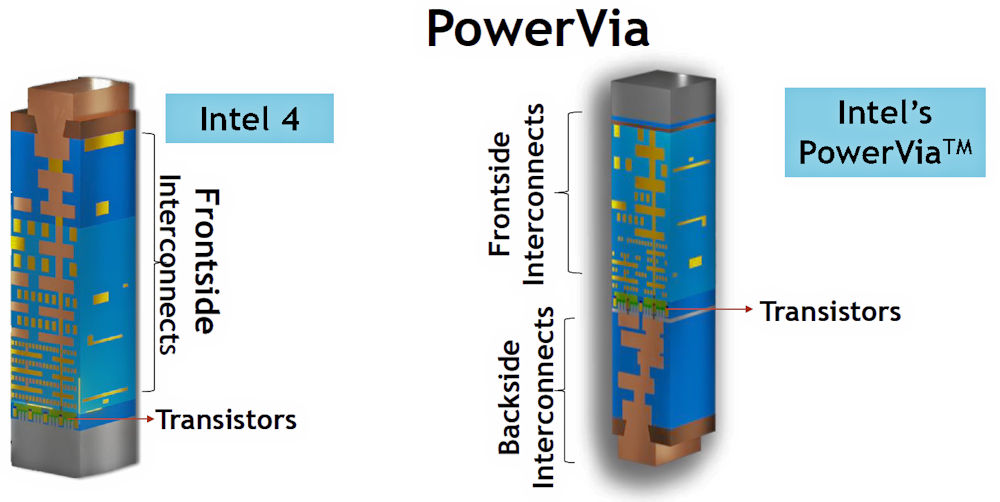
Figure 1: Intel’s PowerVia process moves an IC’s power delivery network (PDN) from the chip’s top metal layers to the backside, which reduces the PDN’s impedance and reduces signal congestion on the top metal layers. Image credit: Intel
Intel presented the results of implementing PowerVia backside PDNs using its Intel 4 process at the recent 2023 Symposium on VLSI Technology and Circuits held in Kyoto, Japan. The results are based on a test chip fabricated using a modified Intel 4 process that integrates multiple x86 efficiency cores (E-cores) running on a 1.1-volt core voltage at 3GHz.
Researchers observed a 30% reduction in IR droop and were able to achieve a 6.7% improvement in maximum operating frequency with the modified Intel 4 process that added a backside PowerVia PDN, compared to an implementation based on the production Intel 4 process without the backside PDN. The team also observed a 20% reduction in signal-wire length on the top metal layers due to the relaxed routing made possible by the backside PDN. The reduced wire length will also help speed the chip’s operation. In addition, Figure 2 shows a 12.5% reduction in the size of a standard cell made possible by the PowerVia PDN technology.
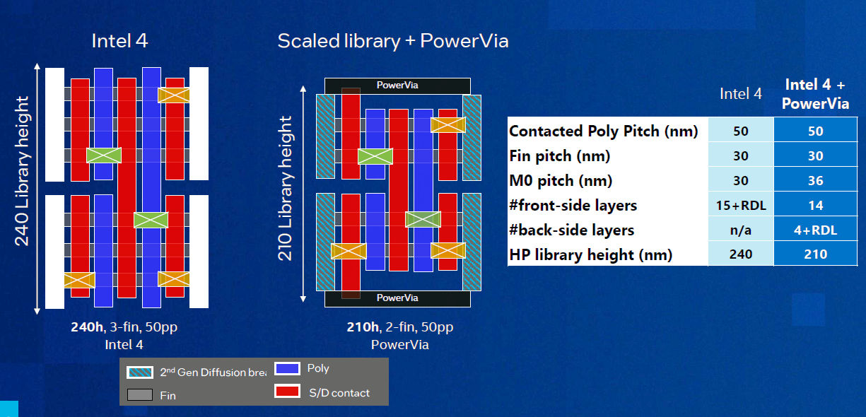
Figure 2: Intel’s PowerVia technology enables the use of 12.5% smaller standard cells when laying out a chip. Image credit: Intel
Figure 3 shows Intel’s plan for introducing the PowerVia technology into its mainstream manufacturing processes. The test chip discussed at the Symposium on VLSI Technology and Circuits employed the existing Intel 4 process with the PowerVia module added, but this is an internal process node and will not be used for mass production. The first production process node that will use the PowerVia technology will be Intel 20A, which will also introduce RibbonFETs – Intel’s name for gate-all-around FETs (GAAFETs). According to Intel, trying out the PowerVia technology on an internal process node reduces the development and production risk for the Intel 20A manufacturing process.
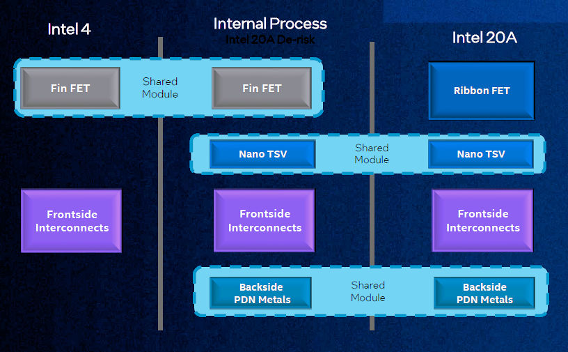
Figure 3: Intel first tested the PowerVia backside PDN on a modified version of its production Intel 4 process and plans to introduce the technology with its Intel 20A production process node. Image credit: Intel
Intel claims that the success it has seen by adding the PowerVia backside PDN to the Intel 4 process jumps it one process node ahead of its competitors with respect to a backside PDN. At its European Technology Symposium held in May, TSMC revealed that it would be introducing a backside PDN with its N2P process node, scheduled for high-volume production in late 2026 or early 2027, so we’ll need to wait a while to see if Intel’s claims prove to be true.
A Fix for All Process Nodes
Instead of developing an improved process node, IP vendor Movellus has evolved its synthesizable Intelligent Clock Network IP to add features that can compensate for voltage droop when used with any process node from any foundry. The evolved concept, called the Aeonic Digital IP Platform, adds voltage sensing in the form of a digital, synthesizable Droop Detector and automatic clock-frequency control to the existing clock-generation network. The original Movellus Intelligent Clock Network distributed a low-frequency reference clock with very precise edges around the chip and then used what the company now calls “Clock Generation Modules” (CGMs) to generate precise, synchronized, high-frequency local clocks. By adding programmable, glitchless frequency shifting and the ability to generate multiple clocks to the clock-module IP produces, Movellus has created a superset of the CGM, which the company calls an “Adaptive Workload Module” (AWM). The current version of this module is called the AWM2. Combined with the Droop Detector, designers can incorporate dynamic voltage and frequency scaling (DVFS) capabilities into their SoCs, using any process node.
Figure 4 shows two ways to incorporate the Movellus AWM2 and Droop Detector IP into an SoC. In the first example, shown at the top of Figure 4, each group of four processing elements shares one AWM2 module (shown in magenta) and one Droop Detector (shown in blue). The lower part of this first example design shows four groups of four processing elements, each with an independent supply voltage and power domain. Each Droop Detector senses the voltage supplied to each group of four processing elements and commands the embedded AWM2 to adjust the operating frequency for those four processing elements. The bottom of Figure 4 shows that one AWM2 module can regulate the operating frequencies for many cores based on the input from multiple droop detectors.
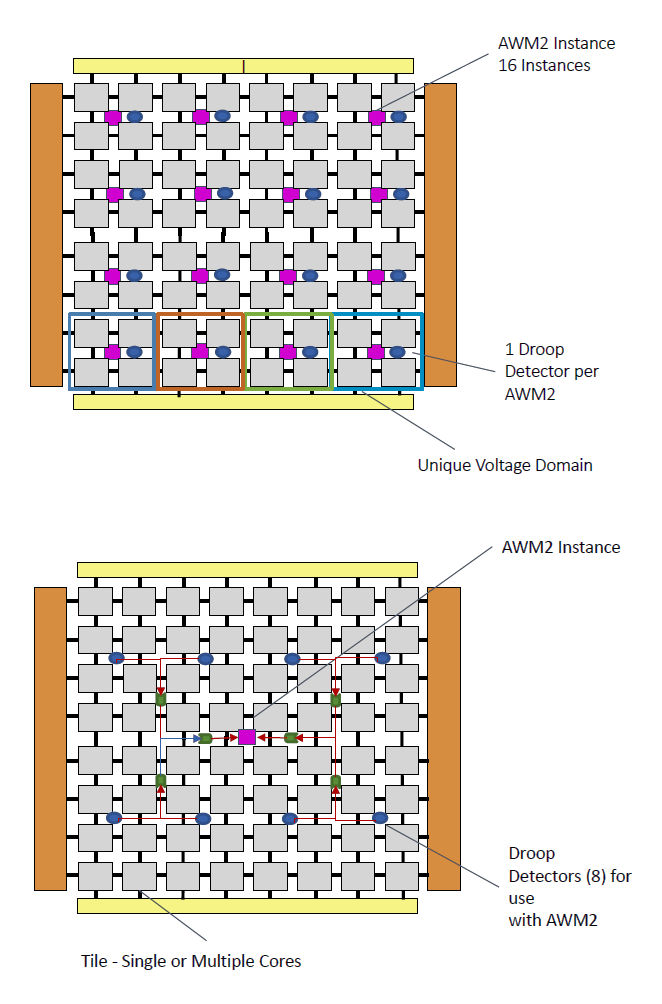
Figure 4: Movellus AWM2 modules can be tied individually to Droop Detectors (top example) or one AWM2 module can take input from multiple Droop Detectors (bottom example). Image credit: Movellus
This Movellus IP allows SoC development teams to potentially get better manufacturing yield, and therefore lower unit costs, from their foundries by allowing wider parametric margins. If the SoC itself can compensate for voltage droop, then supply-voltage margins and frequency guard-banding can be wider. However, development teams will need to adapt this Movellus IP to their designs, which involves learning how to use the IP and developing management software and configurations for the IP. For now, Movellus provides examples and sample firmware, but the company doesn’t currently offer EDA tools to make this task easier. That’s a job that the SoC designers will need to shoulder in addition to the usual PDN analyses.
Voltage droop poses significant challenges for leading-edge SoC designs that employ advanced process nodes and can induce operational faults in some cases. The problem only worsens as chipmakers and foundries chase Moore’s Law down the nanometer rabbit hole and into the angstrom world. Semiconductor manufacturers will need to address these problems, and these examples from Intel and Movellus illustrate that there are multiple solutions to the issue.


