


Network on Chip (NOC) IP has been around for a while. I wrote an article about academic research papers on NOCs presented at the seventh annual International Symposium on System-on-Chip conference held in Tampere, Finland in late 2005. NOCs were the conference’s theme back then and the jury was out on using NOCs to interconnect large IP blocks, including processors, network controllers, and memory on SoCs. NOCs introduce overhead that wasn’t particularly welcome back in 2005. Today, it’s a different story. Interconnect complexity has risen with general SoC design complexity, as you can see in Figure 1.
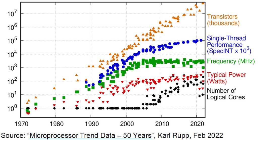
Figure 1: Chip complexity has increased exponentially over the past 50 years, just as predicted by Gordon Moore in 1965.
The orange triangles in Figure 1 show the exponential rise in SoC transistor count in line with the original Moore’s Law prediction from 1965. It’s amazing how consistent this increase has been decade after decade. However, the blue circles and green squares tell a different story. This data, depicting single-thread processor performance and clock frequency graphically depict the death of Dennard scaling. The red triangles show a leveling off of power consumption at around 100 to 200 watts. That’s more a function of the maximum thermal dissipation of the device package.
But the black diamonds in Figure 1 show that, since around the year 2005, the number of IP cores laid down on an SoC has risen dramatically. Consequently, and not shown by Figure 1, the interconnect complexity among these many on-chip cores has also risen dramatically. And that rise has not been just quantitative. It’s not just that there are more interconnects. The role of on-chip interconnect has also grown more complex. It’s no longer sufficient to connect two IP cores with a simple interface so that they can pass data between themselves. There are new considerations, including memory management, cache coherency, data security, encryption, compression, interface translation, and consistency checking to deal with as well.
Because of these changes, the NOC’s time has come. In fact, according to Michal Siwinski and Frank Schirrmeister, respectively the CMO and the Vice President for Solutions & Business Development at Arteris, the inflection point for NOCs really began around 2010 or 2012 with the transition to the 28nm process node, which coincides nicely with the rise in the number of cores per chip shown in Figure 1. That’s when complexity reached the point where NOCs really started to make sense.
NOCs certainly simplify SoC design at the architectural level. To paraphrase an old Tommy Dorsey song, “The Music Goes Round and Round”:
I put the packets through here
The data goes ’round and around
Whoa-ho-ho-ho-ho-ho
And it comes out here
In other words, once you’ve strung the NOC around the chip, packet transfer between IP blocks sort of happens by magic, although I doubt Arteris would agree with that simplification.
However, too much of even a good thing can become a problem and, as the number of IP blocks on an SoC have climbed, so have the challenges of designing with a NOC. Today, an SoC can include four, eight, or more homogeneous or heterogeneous CPU cores, a GPU (graphics processing unit), an NPU (neural processing unit), an ISP (image signal processor), multiple DSPs, several Ethernet and PCIe port controllers, a few USB port controllers, multiple ROM and RAM blocks, and multiple DDR controllers. These IP cores often need to communicate with several other IP cores, especially the memory and I/O blocks. The result is a major traffic headache, which can present a significant challenge when architecting a NOC that meets all of the SoC’s functional requirements.
According to Arteris, today’s most complex SoCs contain multiple NoCs that can consume as much as 10-12 percent of the SoC’s silicon real estate. However, that real estate isn’t contained in one neat bundle. It’s spread all over the chip, as shown in Figure 2.
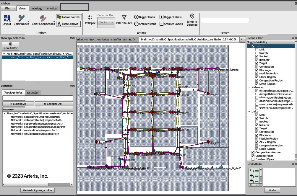
Figure 2: A NOC may need to span the entire SoC, which can present challenges when closing timing. Image credit: Arteris
Because the NOC must stretch completely across the SoC, physical effects – especially delay – become more than noticeable and can prevent timing closure. When timing fails to close, the design goes back to the SoC architect, who often needs to insert NOC pipelines or expand existing NOC pipelines to accommodate the long delays when traversing the great vastness of the SoC. This redesign initiates another design cycle, which may just require a new placement and routing or may force the regeneration of RTL, followed by new gate-level design and a new physical layout. These forced design iterations can take weeks.
Naturally, Arteris now has an answer to this challenge. It’s called FlexNOC 5 and is the latest iteration of the company’s NOC IP. Although there are several new features in this latest FlexNOC incarnation, the big change, according to Arteris, is that the IP is now physically aware. However, this is not a reference to some sort of AI-enabled sentience. Instead, the Arteris Magillem Connectivity tool used to develop NOCs based on the FlexNOC 5 IP has become aware of physical layout information with the ability to read LEF (Library Exchange Format) and DEF (Design Exchange Format) files. As Schirrmeister noted during a discussion, logic synthesis tools gained physical awareness about ten years ago, driven by similar design challenges. Now the Arteris NOC design tools get the same capability.
One more interesting fact arose during my discussion with Siwinski and Schirrmeister. Although we may think of an SoC as having only one on-chip NOC, which might have been true several years ago, today’s more complex automotive, consumer, and enterprise SoCs need to interconnect hundreds of on-chip IP blocks and average 5 to 7 NOCs. Some have as many as 30 NOCs according to Siwinski and Schirrmeister. Those numbers boggle my mind, but they certainly make sense given the block-level complexity that is possible with SoC design in the eras of FinFETs and Angstroms.


Timing closure applies to clocked/synchronous designs/chips. The rest of the world has known for decades/forever: Everything does not run synchronously, so there are synchronizing mechanisms(clock domain crossings?) and various bus flavors.
Sad to say that the pitiful “tool chains” available today have no capability to combine modules to form a system beyond instantiating a module, and absolutely no debug capability.
NO! simulation that just creates waves is just a beginning.
It is sickening that the tools ignore everything that cannot be synthesized(by their own weak kneed tools)
Welcome to the real world, Steve.
Meanwhile on the software side here are compilers, IDEs, and any number of languages in competition.
In myy day we drew block diagrams, second level logic diagrams, pencil and paper simulation, manual synthesis, etc. That was good enough to put men on the moon and bring them back.
It is time to wake-up.
Thanks for the welcome, Karl Stevens, but I am pretty sure I already was in the real world. I’ve worked for EDA and silicon IP companies since 1982 and am pretty familiar with the ebb and flow of design tools for ASIC, SoC, and FPGA design.
Sorry, Steve. I did not mean you personally, rather I meant the EDA tool developers.
I am frustrated because the EDA world keeps doing things the same way over and over expecting different results.
Their attitude seems to be if they cannot synthesize it, then you don’t need it. Meanwhile FSMs and spread sheets are used to try and do what has to be done and they cannot do it.
SystemC, HLS, etc. have been and still are disappointments. There is a better way but there has been so much brainwashing that no one even wants to think about what a poor job the tools do.
For example, timing analysis should not be the first step nor should synthesis. Design first, debug second…
I was one of the first users of EDA and what I see today is not much improved, hence my attitude.
Back then it was a big deal to actually print logic diagrams and generate artwork for printed circuits using a computer. And the tools don’t do much more than that, meanwhile whole systems are being put on chips.