


As I’ve been known to note, one of the great things about being me—in addition to being outrageously handsome, a trendsetter, and a leader of fashion—is that I get to talk to all sorts of interesting companies and people about their uber-cool technologies.
Two related examples spring to mind: the guys and gals at SiMa.ai, whose goal it is to create a machine learning (ML) system-on-chip (SoC) called an MLSoC that can provide effortless machine learning at the embedded edge, and the chaps and chapesses at Arteris IP, whose mission it is to provide state-of-the-art Semiconductor IP and IP Deployment Technology.
Let’s start with SiMa.ai, which was founded in 2018, just four short years ago as I pen these words. The folks at SiMa.ai say that existing ML solutions aren’t purpose-built for the embedded edge, but rather are adapted to it, similar in concept to forcing a square peg into a round hole. Their goal when they founded SiMa.ai was to simplify the process of adding ML to products by delivering “The world’s first software-centric, purpose-built MLSoC platform with push-button performance for effortless ML deployment and scaling at the embedded edge so you can get your products to market faster” (pause to take a deep breath).
In a crunchy nutshell, they wanted to design an MLSoC that could run any computer vision application, any network, any model, any framework, any sensor, and any resolution. More specifically, they wanted to provide users with the ability to solve any computer vision application challenge with a minimum of 10x better performance in terms of frames per second per watt than any competitive offerings while delivering an overall push-button experience in minutes. So, how did they do?
Well, I was recently chatting with Srivi Dhruvanarayan, who is VP of Hardware Engineering at SiMa.ai. As Srivi says, this means that anything to do with the hardware side of the MLSoC—from architecture to logical design to logical verification to physical design to physical verification to bring-up—is his responsibility.
In many ML applications, most of the heavy lifting is performed by a host processor, and only the ML-centric portions of the algorithms are offloaded to an ML accelerator. By comparison, one of the MLSoC’s key differentiators is that it’s a complete system that combines host processor and ML accelerator capabilities in one device. Another key differentiator is that they do all of this at very low power.
If we look at a high-level block diagram of the MLSoC, we see that—in addition to the machine learning accelerator (MLA)—it contains a quad-core Arm Cortex-A65 application processor (AP), a Synopsys EV74 Embedded Vision Processor (EVP) with deep neural network (DNN) accelerator, and… a whole bunch of other IP blocks.
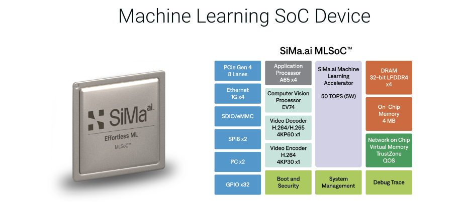
High-level block diagram of the MLSoC (Source: SiMa.ai)
Created at the 16nm technology node, the entire MLSoC comprises billions of transistors. The “secret sauce” to all of this is the MLA, which provides 50 trillion operations per second (TOPS) while consuming a miniscule 5 watts of power.
The simple block diagram shown above reflects only the main IP blocks. It also manages to make things look nice and clean—”easy peasy lemon squeezy,” as it were. The real trick is to connect all of these IP blocks together, which—if you don’t do it right—will end up with your having a “stressed depressed lemon zest” sort of day.
There are three main approaches when it comes to connecting IP blocks inside an SoC. The first is to use a simple bus, where the line marked “bus” in the image below comprises multiple wires to carry any address, data, and control signals.
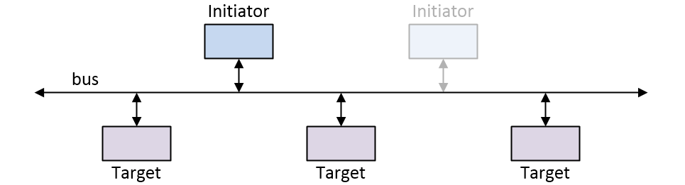
Bus-based SoC interconnect (architecture Source: Max Maxfield)
This bus-based technique is the sort of approach we used back in the 1990s. It’s still applicable to simple designs with only one (or very few) initiator IP block(s) where all of the initiator and target IP blocks support the same interface (i.e., the same bus widths running at the same frequency).
Bus-based interconnect started to run out of steam as designs began to grow more complex, with multiple initiators and lots of targets. One of the main solutions adopted circa the 2000s was to use a crossbar switch-based interconnect architecture.
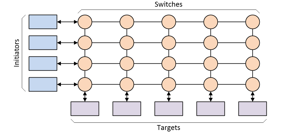
Crossbar switch-based SoC interconnect architecture (Source: Max Maxfield)
As before, each line represents multiple signals. The crossbar switch offers significant advantages, including the fact that any initiator can communicate with any target and multiple transactions can be “in flight” at the same time (the switches have the ability to buffer transactions and determine their relative priority if multiple transactions arrive at the same time).
Unfortunately, like their bus-based ancestors, crossbar switch architectures can do only so much, and they are not able to adequately service today’s high-end SoC designs that feature gaggles of initiators and herds of targets. At some stage, there are so many initiators and targets that connecting them all together results in the interconnect consuming more than its fair share of the silicon, coupled with routing congestion that will bring tears to your eyes (just to be clear, these won’t be tears of joy).
These problems are only exacerbated by the fact that the various IP blocks, which invariably originate with a variety of third-party vendors, may support different interfaces (widths, frequencies, protocols). In the 1990s, an SoC might contain only a couple of handfuls of IP blocks, and the entire device might comprise only 20,000 to 50,000 logic gates and registers. By comparison, one of today’s high-end SoCs can contain hundreds of IP blocks, each of which may comprise hundreds of thousands (sometimes millions) of logic gates and registers.
All of which leads us to the current state-of-the-art in SoC interconnect in the form of a network-on-chip (NoC) (in conversation, “NoC” rhymes with “clock”). Each IP block interfaces with the NoC by means of a “socket,” which handles things like width conversion, protocol conversion, command translation, and clock domain crossing (different IPs can be running at different frequencies).
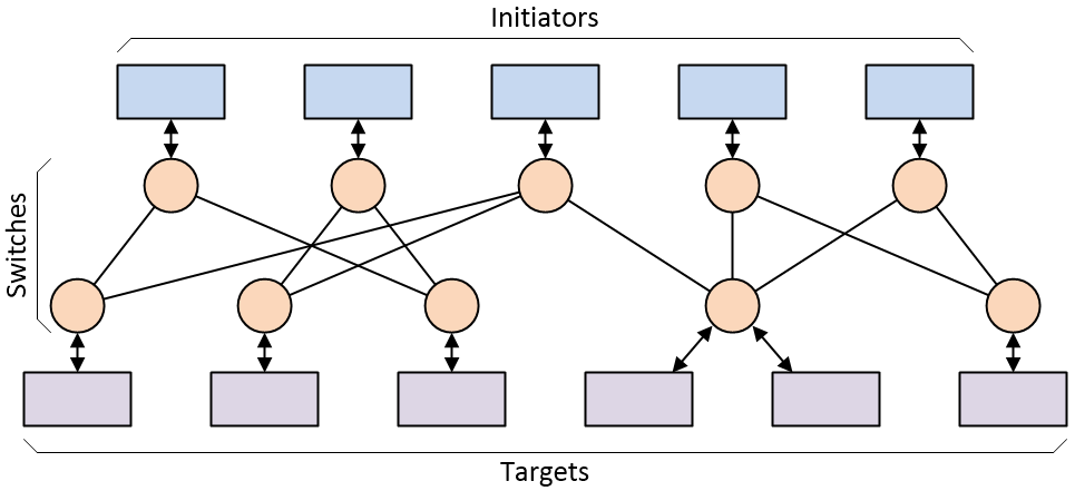
Simple network-on-chip (NoC) interconnect architecture
(Source: Max Maxfield)
Transactions between initiators and targets are sent as “packets,” each of which contains a header (which specifies the destination address) and a body (which contains the request type, data, instructions, etc.). Multiple packets can be “in flight” at the same time, and—once again—if multiple packets arrive simultaneously, the switches can determine their relative priority and buffer lower-priority packets.
As is often the case, this all sounds easy if you talk loudly and gesticulate furiously, but developing your own NoC is a non-trivial task. Srivi told me that he was involved in developing a NoC at his previous company, and that this occupied six to seven people architecting, designing, and verifying that NoC for close to two years.
At SiMa.ai, Srivi wanted his team to focus on the design of the MLA and implementing the MLSoC. Thus, he started looking around to see what was available in the form of powerful, flexible, and robust NoC IP that would allow the team to seamlessly connect IP blocks from many different sources with many different interfaces. It didn’t take long before Srivi was introduced to FlexNoC Interconnect IP from Arteris.
As a simple rule of thumb, irrespective of whether the IP blocks in the design employ a mix of AMBA AXI3, AXI4, AHB, APB, OCP, PIF, or proprietary protocols, Arteris FlexNoC IP reduces the number of wires by nearly one half (as compared to the next-best interconnect strategy), resulting in fewer gates and a more compact chip floor plan (this may explain why Arteris system IP is currently used in over 70% of today’s automotive SoC designs).
One of the great things about FlexNoC is that it allows the SoC developers to explore the solution space by quickly and easily evaluating different NoC implementations (e.g., one large NoC vs. multiple smaller NoCs). FlexNoC also comes equipped with a handy-dandy performance analysis capability that helps the developers to determine if their various “pipes” and “highways” are big enough and fast enough to achieve their performance goals.
“The proof of the pudding is in the eating,” as the old saying goes. Well, from what I’ve heard, a metaphorical pudding filled with FlexNoC would be a tasty treat indeed. As Srivi says, “Our company was formed in 2018, we designed what is arguably one of the most complicated SoCs on the planet in just over three years, we taped out in February 2022, and we received our first silicon in May 2022, all thanks to our amazing partners like Arm, Synopsys, and Arteris. With zero bugs, we continued our march towards first-time-right success by going straight into production. Just six weeks after receiving first silicon, we were working in our customers’ labs running their end-to-end application pipelines and knocking their socks off with the 10X advantage we had promised to deliver.”
Full disclosure: I’m not planning on developing a multi-billion-transistor SoC myself anytime soon. If I were, however, a NoC would form a key element of my design, and I think it’s reasonably safe to say that this NoC would be realized using FlexNoC Interconnect IP from Arteris. What say you? Are you currently involved in designing SoCs? If so, how are you addressing your own on-chip interconnect challenges?


