


As discussed in Parts 1 through 4 of this article series, the earliest PLDs evolved along easily traced genetic lines that started with Harris Semiconductor’s programmable diode arrays from the 1960s and progressed through bipolar PROMs, the Signetics 82S100 FPLA, MMI’s PALs, and finally the transcendent CMOS replications of PAL devices created by Altera and Lattice Semiconductor. By contrast, FPGAs (called “Logic Cell Arrays” in the first press release) came from a similar concept, field-programmable logic, but from an entirely different direction.
While working at microprocessor pioneer Zilog in the early 1980s, an engineer named Ross Freeman conceived of a new logic circuit that was reprogrammable: a single piece of silicon that could meet the logic-design needs of ASIC customers, but with instant turnaround on the design. At that time, there were dozens, perhaps hundreds, of ASIC companies designing and building custom silicon for thousands of customers. However, designing and fabricating ASICs took many months. Freeman’s idea would permit the development and implementation of a custom IC in less than a day.
Freeman earned a BS degree in physics from Michigan State University in 1969 and a master’s from University of Illinois in 1971. He worked in the Peace Corps and taught math in Ghana for two years, and then joined Teletype Corporation where he got some PMOS design experience. Freeman was one of the first engineers to join Federico Faggin’s new microprocessor startup named Zilog, where he designed the Zilog Z80-SIO chip. Freeman was the Zilog Components Division’s Director of Engineering by the time he reached his early 30s.
Freeman conceived of a new type of hardware-programmable device – destined to become the world’s first FPGA – while working at Zilog. He filed several patents, but Zilog was not interested in pursuing the concept. Freeman decided to start his own semiconductor company to pursue the FPGA concept and convinced Jim Barnett, a Zilog coworker, to join him. The two of them persuaded Bernie Vonderschmitt, an experienced electronics and semiconductor executive working at Zilog, to become the startup’s CEO.
Vonderschmitt had spent more than three decades at RCA Corp before he joined Zilog. He headed RCA’s color television development in 1953 and eventually became the Vice President and General Manager of the company’s Solid State Division, which had developed COSMOS (RCA’s trade name for CMOS). Seiko executives visited RCA’s Solid State Division seeking a license for RCA’s COSMOS process technology to help jumpstart its electronic wristwatch business. Vonderschmitt licensed RCA’s COSMOS process to Seiko Epson, and by 1973, the company started selling Seiko digital LCD wristwatches based on CMOS chips made by Seiko Epson.
While serving as the head of RCA’s Solid State Division, Vonderschmitt got a clear-eyed view of semiconductor manufacturing’s voracious appetite for capital, driven by the need to upgrade process technology every couple of years to keep pace with Moore’s Law. Companies that failed to invest in their fabs quickly dropped out of the game.
Vonderschmitt often had trouble obtaining needed capital from the parent corporation to scale new IC process technologies for production, largely because chip making was always just a side hustle for RCA. The company preferred making consumer and broadcast equipment. Based on his experience with RCA’s Solid State Division, Vonderschmitt decided that captive semiconductor fabs were just too expensive and too burdensome. “If I ever start a semiconductor company, it will be fabless,” he vowed.
Vonderschmitt, Freeman, and Barnett officially founded Xilinx in February 1984. Vonderschmitt planned to focus Xilinx on designing innovative programmable devices and partnering with other companies to gain access to capital-intensive chip manufacturing. He leveraged his decade-long friendship with a Seiko Epson executive named Saburo Kusama and enlisted his help in getting Seiko Epson to manufacture Xilinx FPGAs.
The task of actually designing the first FPGA fell to an engineer recruited from Zilog named Bill Carter. Freeman had originally hired Carter to work on the Zilog Z8000 microprocessor project. As frequently happens in Silicon Valley, Carter quickly followed Freeman to Xilinx to work on FPGA designs. He had previous bipolar and MOS IC design experience, but Seiko Epson’s process technology was CMOS. The Xilinx FPGA would be his first CMOS chip design.
Like all FPGAs that followed, the first FPGA would be a very large chip. Vonderschmitt regularly advised Carter to keep the design as simple as possible and to not try anything “too clever or exotic.” Minimizing design risk was very important to Vonderschmitt. He realized that a tiny startup offering a first-of-its-kind chip that required unfamiliar design tools and was fabricated through a unique fabless business model could easily scare off customers.
Seiko Epson’s CMOS digital watch chips employed very conservative design rules to maximize yields and drive down costs, because the watch business is very price competitive. Digital watch chips are slow. Really, really slow. They run at 32KHz. The first Xilinx FPGA design would not be conservative and it would not be slow. Xilinx was shooting for clock rates in the tens of MHz.
The first FPGA’s architecture was largely based on one modular CLB (configurable logic block) and one modular I/O block, repeated many, many times. Repetitive use of identical modular blocks greatly simplified the FPGA’s design, which was essential, considering the small design team and minimal design tools available to the startup. The situation is strikingly similar to Intel’s beginnings in 1968. Robert Noyce and Gordon Moore founded Intel to be a memory company, because memory chip designs repetitively use the same memory cell over and over again, which yields a relatively complex chip with minimal design costs.
Carter’s finished FPGA design required approximately 85,000 transistors to implement its 64 configurable logic blocks and 58 I/O blocks. The 16/32-bit Motorola 68000 microprocessor needed fewer transistors. The FPGA’s die size would be larger than almost any chip being manufactured at that time, and it would certainly be a much bigger chip than anything Seiko Epson had ever fabricated.
The first Xilinx chip taped out in late May 1985, and the design team had to wait two more months, until early July, for first-run silicon. Seiko Epson sent a box containing 25 finished wafers. The first ten wafers out of the box were completely dead. All had solid power-to-ground shorts. Not a good start. The eleventh wafer showed some signs of life but exhibited very high current draw. The last fourteen wafers were also completely dead. They, too, had short circuits between power and ground.
Carter’s team discovered that there were aluminum whiskers covering all of the first-run wafers. A poorly etched aluminum metallization layer shorted out the power and ground rails. Fortunately, the metal whiskers on the wafer that was only partially dead were tenuous enough to blow like fuses. (The first FPGA was not designed as a fuse-programmable device, but a flawed manufacturing process made it one.) The test team managed to vaporize the whiskers by driving a massive amount of current into the wafer. It was a risky gamble, but there was little to lose.
With the shorts cleared, Carter was finally able to clock a simple configuration bit stream into a device. He successfully programmed an inverter into one of the CLBs. Carter immediately called Freeman and Vonderschmitt while they were traveling in Japan, reporting that the “DONE line had gone high,” which signified that Xilinx “had successfully created the world’s most expensive inverter.” After this initial success, the design team was able to program more and different logic circuits into the FPGA.
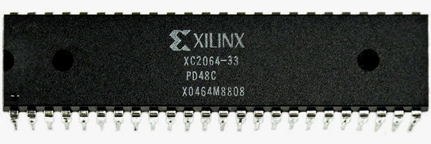
A press release dated November 1, 1985 announced the Xilinx XC2064, the world’s first “Logic Cell Array.” That was the FPGA’s original classification, but the device was destined to be called an FPGA. Here’s a photo of the Xilinx XC2064, packaged in a 40-pin DIP:
Strategically, the press release didn’t position the Xilinx XC2064 as a PLD. It called the device a new type of ASIC. This wording reflects Xilinx’s orientation towards the higher end of logic programmability. “Logic cell arrays provide all the benefits associated with other ASICs – reduced chip count, high performance, smaller system size, lower power consumption and high reliability – with none of the time, cost and risk penalties,” proclaimed the press release. The second page of the release stated “Logic cell arrays use a gate array-like architecture.”
The press release then puts even more distance between the new Xilinx FPGA and existing PALs and PLDs:
“The device is therefore comparable to smaller gate arrays and provides higher complexity than do programmable array logic type (or ‘PAL-type’) devices, which typically offer from 150 to 300 equivalent gates. The XC2064 can take the place of smaller gate arrays; 15 to 75 SSI and MSI (small- and medium-scale integration) devices; or four or more currently available PAL-type devices.”
Despite these advantages, FPGA adoption came slowly, unlike the rapid adoption that MMI’s PALs experienced in the late 1970s. That’s because John Birkner and MMI made sure that PALs were very easy for system designers to incorporate into their existing design methods: PALs were fast; they were simple and easy to understand; they fit well with existing TTL-based design techniques; and an individual PAL cost a little more than a TTL chip, but it didn’t cost a lot more.
The Xilinx FPGA was an entirely different beast. Like an ASIC, the FPGA was considerably more complicated than a PAL and therefore harder to understand and more difficult to use. FPGA design tools were completely unfamiliar to most design engineers, just like ASIC design tools. No one knew how to work with FPGAs, at first. Early FPGAs were slow compared to TTL and PAL devices. The XC2064 FPGA couldn’t replace all that much logic with only 64 CLBs. Certainly not as much as a masked gate array. The huge CMOS die that Seiko Epson had struggled to manufacture meant that Xilinx needed to charge a premium price for its FPGAs to get any sort of profit margin.
And yet, despite all of these obstacles, FPGAs have succeeded. Over the next twenty years, more FPGA vendors entered the market, targeting and assimilating nearly every other digital function typically found on a circuit board, including SRAMs, level translators, DSP engines, Ethernet and other high-speed serial transceivers, and finally, entire microprocessors. Over time, FPGA offerings stratified into high-end, mid-range, and low-cost product lines. As FPGA choices diversified and as the devices vacuumed up more and more digital functions from other chips typically used on most circuit boards, engineers increasingly embraced FPGAs. After nearly four decades on the market, FPGAs are now widely used.
The IEEE listed the Xilinx XC2064 as one of the “25 Microchips that Shook the World” in 2009 and inducted it into the Chip Hall of Fame in 2017.
Note: The evolution and diversification of the FPGA after its 1985 debut is a large and complex story unto itself. That story requires its own article series.
Stay tuned.


Hi Steve, Awesome article series! Well told! Thrilling read, capturing the essence and excitement of the epic growth of programmable logic.
I am staying tuned for the evolution and diversification of the FPGA.