


By the end of the 1970s, PALs had become the PLD (programmable logic device) of choice for system designers. They were an immensely successful product for Monolithic Memories Inc (MMI). They were also a great target for every other IC maker that wanted to enter the PLD arena. Several did just that.
Bob Hartmann co-founded Source III in 1980. The consultancy specialized in the design of gate arrays, because the early 1980s was definitely a golden time for gate-array development. The major gate-array vendors of the day – including LSI Logic, Signetics, Intersil, AMI, and Fujitsu – provided master slices and tools. It was the customer’s job to create the design using the vendor’s tools. Source III acted as an experienced intermediary. This work prompted Hartmann and his fellow consultants to wonder if there wasn’t an available niche for a PLD to replace some of the gate arrays being developed, given the difficulty, NRE expense, and time needed to develop a gate array.
In an oral history taken by the Computer History Museum with several founders and early Altera employees – Yiu-Fai Chan, Robert Frankovich, Robert Hartmann, Clive McCarthy, and Don Wong – Hartmann described the thought process that resulted in the founding of Altera in 1983:
“Having done that for a couple of years, then seeing how the problems of making that kind of design system work, and the difficulties of it, and the cost of having to produce custom mask sets, to do a particular part type, all of these problems. We had the notion, in a survey book that we wrote, wouldn’t it be wonderful, basically, if somebody could come up with something that is programmable after it was manufactured to do general-purpose logic. We felt that it would be a game-changer. So, subsequent to that, we said, ‘Hey, why don’t we see if we can launch off in this direction?’ And that’s what we did.”
Hartmann raised $750,000 to start Altera in the company’s first funding round. That wasn’t enough money to get a chip design, but it was enough to make a start. The venture capitalists wanted Altera to develop a test chip. Hartmann wanted to leave the starting gate with a large design that could directly compete with some of the gate arrays on the market. Robert Frankovich, who’d met Hartmann while working at Fairchild Semiconductor in the 1970s and had subsequently joined Hartmann’s Altera, felt that Altera’s first design should be a minimum viable product that could be sold: not a test chip, which would take nearly the same effort to design as an actual product and would result in nothing more than a proof of concept, but not a large PLD either.
Frankovich won the argument and surveyed the landscape, looking for a “killer app,” a successful, easy target that they could steal business from. At the time, the most successful PLD family on the market, by far, was MMI’s 20-pin PAL family (extensively discussed in Part 3 of this article series), so of course, PALs became the primary target for Altera’s first PLD design.
Like the other successful PLDs on the market in 1983, MMI’s PALs employed bipolar technology with metal fuse programming, which resulted in the fastest parts. Altera wanted to take a different direction. Frankovich knew that not everyone wanted the fastest possible part. He also knew that bipolar technology wouldn’t scale to larger devices because of the power consumption and heat dissipation. Altera’s first PLD would compete with PALs, but subsequent devices would compete with gate arrays and would therefore need to grow much larger.
Altera’s team chose a CMOS EPROM process as the implementation technology for its first PLD, which was about as radical a departure from a bipolar IC with metal-fuse programming as you could get. This choice of process technology had multiple benefits:
- It could be used to make far bigger devices
- It was erasable
- It would draw far less power
The ability to make larger devices would allow Altera to chase the market currently served by gate arrays. Erasability meant that systems designers (like me) would not end up with a paper cup full of expensive, used PLDs on their bench to serve as a reminder that design errors cost money. And of course, everyone likes lower power consumption. The one drawback, slower propagation delays, meant that Altera’s PLDs would not solve everyone’s design problems. However, no IC ever does.
Very few chipmakers had a CMOS EPROM manufacturing process. The only company with such a process that was willing to work with a small startup like Altera was Ricoh, in Japan. So Ricoh became Altera’s first foundry, and Altera can claim with some authority that it was the first truly fabless chip vendor.
Process technology was only the first hurdle. The second challenge was packaging. EPROMs are packaged in wide DIPs with quartz windows to allow ultraviolet light to enter the package and erase the EPROM cells. Because Altera was planning on competing with 20-pin PALs, the company needed a skinny, 20-pin package with a quartz window. No such package existed at the time, so Altera had to get one tooled as a custom package.
Altera had opened its doors in June, 1983. The company had taped out its first PLD, the EP300, by Christmas of that year: less than 6 months to tape out the first chip. The EP300 development team consisted of six design engineers (Yiu-Fai Chan, Haugh Suo, Robert Hartmann, Jim Sansbury, John Oh, and Don Wong) and four layout designers (Bob Frankovich, Mark Belshaw, Susan Falk, and Kathy Hopkins). That’s the sort of thing that was possible back then. You could gather a handful of engineers, set up shop in a Silicon Valley office building, design a chip, tape it out, and be ready to make masks in half a year. Things were simpler back then. Altera introduced the EP300 EPLD (erasable PLD) in July, 1984.
At the time, MMI offered seven different versions of its 20-pin PALs. One Altera EP300 could replace all of the members of MMI’s 20-pin PAL product line, and more. You could program the same Altera EP300 to emulate any of the seven MMI 20-pin PALs, because MMI had designed its PALs in a modular, mix-and-match fashion using several different macrocells. Some of these PAL macrocells included 1-bit output registers and others did not. You could mix and match these macrocells in an EP300 design and create PAL configurations that MMI didn’t offer – all with the same Altera EPLD.
As long as you didn’t need the speed. The CMOS EP300’s input-to-output propagation delay was 90 nanoseconds. MMI’s bipolar PALs were more than four times that fast.
As it turned out, not everyone needed the speed, and Altera quickly started selling lots of EPLDs. MMI had prepared the market and Altera’s EP300 hit its target dead center. Altera started generating positive cash flow within two years of its founding. It got the chance to build those bigger and bigger devices to start competing with gate arrays. The Altera EP300 device held about 300 gates worth of logic in eight macrocells.
MMI’s market success with PALs attracted Altera’s attention, and it attracted another competitor: Lattice Semiconductor. Founded in Hillsboro, Oregon in 1983, Lattice also copied the MMI PAL device architectures with its GAL (Generic Array Logic) 16V8 device. Like Altera, Lattice chose to fabricate its PAL alternative using a CMOS process technology. Unlike Altera, Lattice chose an electrically erasable CMOS (E2CMOS) process that provided more on-chip device density and allowed the devices to be erased electrically. This feature permitted 100 percent testing of the manufactured 16V8 devices prior to shipping. Lattice could load the packaged GALs with multiple test patterns and then completely erase them after final testing.
Lattice’s GALs were significantly faster than Altera’s EP300 EPLD. With a 15 nanosecond input-to-output propagation delay, they were faster than MMI’s bipolar PALs, too. (Lattice emphasized this fact in marketing literature and with the phone number for its application hotline, 1-800-FASTGAL, prominently featured at the bottom of every other page in the Lattice Generic Array Logic Handbook.)
GALs consumed less power than bipolar PALs because Lattice made them using a CMOS process technology. Like Altera’s EP300 EPLD, one 20-pin Lattice GAL could emulate any of MMI’s 20-pin PALs, which reduced the number of blank devices an OEM system vendor needed to keep in inventory. That was a cost-reducing advantage for GALs. Because of all these advantages, Lattice’s GALs quickly gained market share in the PAL arena.
Lattice introduced its GAL 16V8 PLD in April, 1985, less than a year after Altera’s EP300 EPLD hit the market, and Lattice immediately started spreading FUD (fear, uncertainty, and doubt) about Altera’s approach. Here’s what the 1986 Lattice Generic Array Logic Handbook had to say about an unnamed, competing product based on ultraviolet-erasable CMOS (UVCMOS) process technology:
“UVCMOS addresses many of the shortcomings of the bipolar approach, but introduces many shortcomings of its own. This technology requires much lower power and, while it has the capability to erase, this comes at the expense of slower speeds and cumbersome erase procedures.”
FUD-based marketing was, is, and likely will always be a hallmark of programmable logic marketing. Lattice didn’t invent FUD. It’s been a part of technology marketing for many decades, and a key component of automobile marketing for decades before that.
Meanwhile, AMD had become an alternate source for MMI’s PALs by licensing the PAL patents in late 1980 or early 1981. Being an alternate source was a bread-and-butter business for AMD. Because the agreement was for patent use, not masks, AMD designed its own PALs, using its own semiconductor technologies, and improved on MMI’s parts. For example, instead of using titanium-tungsten fuses, as MMI had in its original PALs and PROMs, AMD had a more reliable platinum silicide fuse from its own PROM designs, which improved programming yields. Although customers could return the MMI PALs that didn’t program correctly to the factory for credit, this process increased costs, required additional accounting effort, and it just irritated MMI’s customers in general. AMD’s salespeople exploited this situation and could outsell MMI just by emphasizing this one advantage over MMI’s PALs.
This alternate-source arrangement for PALs allowed AMD salespeople to speak with many PAL customers about their needs. Engineers would pull out their schematics and show AMD’s salespeople exactly how they were using the existing parts. They’d talk about the PALs’ shortcomings and the additional features they’d like to see. This was great, in-depth market research.
One of the shortcomings uncovered by this research was the continual shortage of PAL inputs and outputs that engineers experienced with their PAL-based designs. It seems that the chosen PAL, whichever was chosen, was always one or two input or output pins short. Or one of the outputs needed a register and didn’t have it. As a result of this grass-roots market research, AMD was able to define and develop a bigger, better PAL called the 22V10, which was still a bipolar part, but it had more input and output pins, and it incorporated more output macrocells (10 instead of 8). The 22V10 was packaged in a larger, 24-pin package to accommodate the additional input and output pins.
AMD introduced 22V10 in June, 1983 and it became an overnight success. It was familiar, because it was a PAL, but it offered that little bit more that engineers craved. Altera responded to AMD’s 22V10 introduction by developing and announcing the EP600 EPLD in July, 1985. The Altera EP600 emulated the 22V10 PAL in the same way that the pin-compatible EP300 emulated MMI’s 20-pin PALs. Altera figured lightning might just as well strike twice. (Lattice also developed a GAL 22V10.)
However, the EP600 was not Altera’s second EPLD. Altera introduced its second EPLD, the EP1200, in October, 1984. The EP1200 packed about 1200 gates worth of logic in 48 macrocells and was packaged in a 40-pin DIP. Larger PLCC and PGA packages allowed the same EP1200 die to support even more input and output pins. The EP1200 EPLD leapt far beyond the abilities of any PAL, heading towards gate-array territory, but with a field-programmable device. Its gate capacity was significantly smaller than any gate array, but it demonstrated that Altera was headed in the right direction. The photo below shows an Altera EP1200 EPLD mounted in a 40-pin DIP.
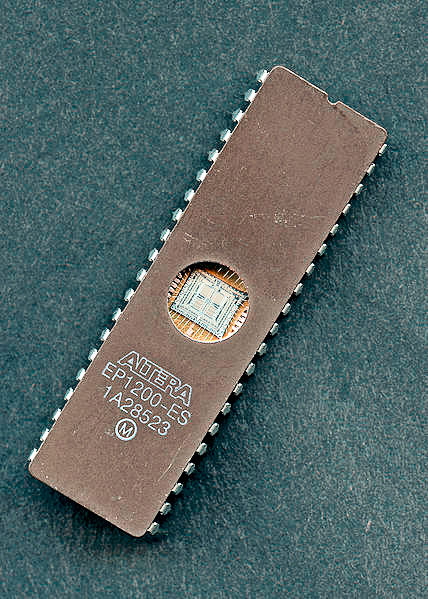
Altera EP1200 EPLD mounted in a 40-pin DIP. Image Credit: Michael Holley
(Note: Altera’s EP600, EP900, and EP1200 EPLDs are uniquely distinguished by appearing in the premiere issue of Michael Slater’s The Microprocessor Report, in September, 1987. It was a dubious honor because Slater’s specialty, honed at Asilomar Microcomputer Workshops before he founded The Microprocessor Report, was collecting and discussing chip errata. Consequently, Slater’s short EPLD article, which appears in the “Bugs and Quirks” section in the premiere issue of his newsletter, says: “Altera’s EP600, 900, and 1200 devices have an automatic standby mode which is initiated whenever all inputs have not changed for approximately 100 ns. This feature is designed to save power when operating with slowly changing inputs. Unfortunately, if the device is in standby mode, glitches may occur on combinatorial outputs when related inputs change. So, unless your system is fully synchronous and can tolerate glitches on the EPLD’s outputs, set the ‘Turbo’ bit to prevent the chip from ever going into standby mode.” Helpful advice, but something tells me Altera didn’t appreciate the publicity, although I might be wrong about that.)
Eventually, marketers working for programmable-logic vendors stopped calling their larger programmable-logic devices “PLDs” and inflated the term to “CPLDs” (complex PLDs). CPLDs continued to mimic the original macrocell organization in MMI’s PALs; they just had more inputs and outputs and incorporated more macrocells. Logically, CPLDs are a bunch of PAL macrocells, placed on the same chip, and all wired together.
If you were expecting Altera to become an FPGA vendor in this article, that won’t happen until Altera introduces its first FPGA, the Flex 8000, in 1992. Altera quickly replaced the Flex 8000 FPGA with the Flex 10K family, which were the first FPGAs to incorporate embedded RAM blocks. Altera’s Flex 10K family was quite successful, but that’s not part of the CPLD story. At first, Altera was so wary of Xilinx’s FPGA patents that it referred to the Flex 8000 and Flex 10K devices as “LUT based PLDs” instead of FPGAs. However, this no longer seems to be an issue, three decades later.
FPGAs offer many advantages and benefits over PALs, other smaller PLDs, and CPLDs. I’ll discuss the history of the first FPGA in the final chapter of this article series, next week.
Stay tuned.
References
Altera EP300 Design & Development Oral History Panel, Computer History Museum, August 20, 2009.
Oral History of Don Faria, Computer History Museum, October 16, 2017.
Advanced Micro Devices (AMD) 22V10 Programmable Array Logic (PAL) Development Team Oral History Panel, Computer History Museum, July 19, 2012.
I.C. Startups 1987: The Next Generation, Dataquest Semiconductor Industry Group, 1986.


One thought on “How the FPGA came to be, Part 4”