


I’m about to wax eloquent on a new generation of optical switches that are poised to revolutionize the communication capacity and performance of data centers—especially the AI and hyperscale flavors (ooh, tasty—and very real, as operators like Google have already proven)—while also cutting power by 40%, but first…
The phrase “It’s a funny old world, and no mistake” is an informal, colloquial British English expression used to comment on life’s unexpected, unusual, or contradictory events. I remember the ancient ones muttering this mantra to themselves when I was a lad. I wish I could get my chronal conveyance working and go back in time to tell them they were right.
For example, whenever I publish a column, I post a link to it on LinkedIn. Earlier this week, I posted a column titled Monetizing Stranded Megawatts in AI Data Centers. The thrust of that column was that the real constraint on AI’s growth is no longer silicon, but power—and that smarter orchestration of existing power capacity may matter more than faster chips.
Apropos of nothing at all, since I’m prone to meandering musings, I also mentioned that my mum was gifted with a doll for Christmas when she was five years old, that her younger sister accidentally broke it, and that my wife (Gina the Gorgeous) recently replaced it.
Wouldn’t you believe it? I’ve received more missives about my mum and her doll than about the monetization of unfulfilled megawatts, even though the latter is of great import to the owners and users of AI and hyperscale data centers. It truly is a funny old world, and no mistake.
Actually, since we’re here, I got off a FaceTime call with my mum just prior to penning these words. For some reason, I mentioned that my grandad and grandma (my mum’s parents), who passed many years ago, would not believe their eyes if they could see the two of us having a video conversation 4,000+ miles apart.
Mum reminded me that they didn’t get electricity in their house until 1940, when she was 10 years old (they only got it so they could listen to the radio to find out what was going on in WWII). She said that my grandparents simply wouldn’t have understood concepts like iPads, Wi-Fi networks, and video conferencing. She also repeated something she’d told me before: that my grandma would have been amazed to see something like an electric tea kettle or an electric toaster. We both had a bit of a chuckle, during which I took a sneaky screenshot, as seen in the image below.

But we digress… returning to the topic at hand, I’ve just been introduced to some incredibly interesting optical switching technology that could revolutionize the communication capacity and performance of data centers.
Before we plunge into the fray with gusto and abandon (and aplomb, of course), let’s first set the scene. One problem we have is that the terminology pertaining to data centers is evolving as we speak. In the early days, circa the 1990s, we talked about data centers with racks, and racks with servers. Around the beginning of the 2000s, we also started talking about thin servers called blade servers, or blades.
In those days of yore, virtually all intra-rack interconnects (i.e., communication between servers or blades in a rack) and inter-rack interconnects (i.e., communication between racks in data centers) were electrical. This involved copper backplanes or cables and electrical packet switches connecting servers and racks. Electrical links dominated because they were cheap and well-understood, and speeds were low enough that copper could handle both intra-rack and short inter-rack interconnects with acceptable power and signal integrity.
As network speeds pushed past 40 Gb/s and into the 100 Gb/s+ range, optical inter-rack links became mainstream starting roughly in the mid-2010s. In contrast, intra-rack links (within a rack or between switches inside a rack) stayed mostly electrical (high- speed copper) for cost and practical reasons through much of the late 2010s and early 2020s.
Alongside all this, underlying processing technologies were evolving. In the early days of data centers, throughout the 1990s and the early 2000s, virtually all servers used only central processing units (CPUs) for general-purpose computing.
Graphics processing units (GPUs) were originally designed in the 1990s for graphics and 3D rendering. They began appearing in server environments in the late 2000s and early 2010s because their highly parallel architecture made them well-suited for data-parallel workloads. This was especially true in the case of scientific computing and, later, artificial intelligence (AI), machine learning (ML), and high-performance computing (HPC).
The mid-2010s saw the introduction of neural processing units (NPUs). These are AI-centric processors that are designed to perform neural network computation with very high efficiency. It’s also common to hear talk of tensor processing units (TPUs). These were designed by Google and deployed in Google’s data centers.
In fact, TPUs arrived on the scene before NPU became a common term. The way I think about this is that a TPU is a specialized form of NPU—one that helped define the category before the category had a name.
These days, it’s common to use the term “XPU” to mean “Some kind of processing unit, where ‘X’ is a placeholder for the specific type.” That is, XPU is an umbrella term encompassing CPUs, GPUs, NPUs, TPUs, and other “PUs” of that kind.
One more thing before we proceed is that the Open Compute Project (OCP) and hyperscalers commonly talk about “compute nodes,” meaning servers, blades, or accelerator modules containing XPUs, memory, and local I/O. The term “sled” is a form- factor implementation of a compute node.
As before, racks contain multiple sleds or servers, along with top-of-rack (ToR) switches. Also, the relatively new term “pod” refers to a group of multiple racks with a defined internal network topology. Pods are designed to be replicated. The way to think about this is that compute nodes live in sleds, sleds live in racks, racks live in pods, and pods live in data centers (phew!)
As we noted earlier, intra-rack links (within a rack or between switches inside a rack) remained mostly electrical through much of the late 2010s and early 2020s. The first outlier was Google, which introduced intra-rack optical links along with its TPUs. That is, the TPUs themselves transmit and receive data over optical fibers.
As a result, Google reported up to 40% power savings and around 30% cost reductions at the full data-center level for large-scale AI training and inference workloads. And to be clear, this “40% power reduction” isn’t confined to the interconnect—it applies to the entire data-center energy footprint.
That’s a staggering improvement, especially when several analyses (including IEA forecasts) indicate that global data-center electricity consumption could top 1,000 TWh per year by 2026, after which growth is expected to accelerate dramatically.
The problem is that, while Google’s optical switches are state-of-the-art, they aren’t actually as good as one might hope. Consider a Google optical circuit switch (OCS) as depicted in the diagram below.
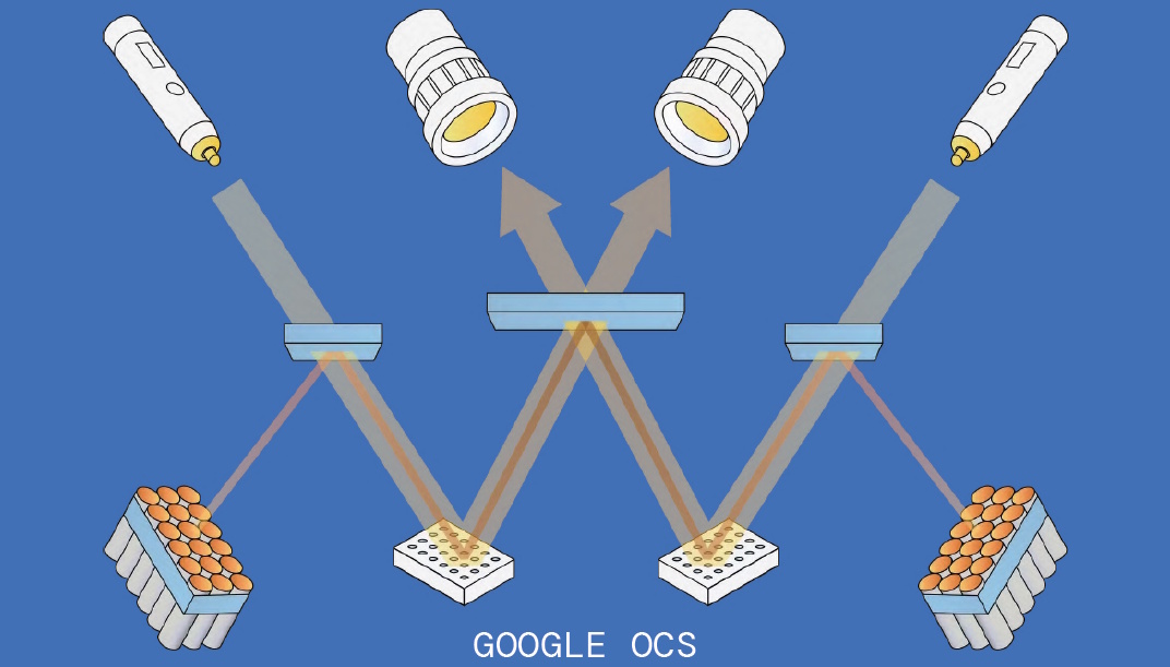
Google OCS (Source: Omnitron Sensors)
This takes a bit of wrapping one’s brain around, so let’s take it step by step. There are two bundles of optical fibers in the bottom-left and bottom-right corners. Each fiber, which is referred to as a channel, can transport bidirectional optical data.
The white blocks with little circles in the bottom-middle are the MEMS mirror arrays (the active, steerable elements). The blue rectangles in the middle of the drawing represent static partially reflective mirrors.
The MEMS mirrors can be controlled so that light from any channel on one side can be routed to any channel on the other side. This is an incredibly dynamic process, with input-to-output paths being reassigned on the fly.
The problem with Google’s implementation is that, by default, they don’t know exactly where the active steerable MEMS mirrors are pointing. This explains the “illuminators” in the top-left and top-right corners of the above diagram. These act like 850-nanometer- wavelength “flashlights” whose light passes through the partially reflective static mirrors, bounces off the MEMS mirrors, and is viewed by cameras. A sophisticated feedback system continuously reevaluates and corrects the positioning of each mirror.
Just to make life really exciting, this switch, which is about the size of three Rubik’s cubes stacked in a row, has stability issues. For example, if someone walks by the racks, or if a pump or a fan turns on or off, the ensuing vibrations can result in short interruptions and glitches in the data because the mirrors are bouncing around.
Last but not least, there is a limit on the number of channels per switch. As part of its Apollo project, Google built a 136-input-by-136-output non-blocking optical switch. Many such switches are combined to support thousands of optical channels in a large AI pod and tens of thousands in an AI data center.
In one of their own white papers, the folks at Google listed four challenges that they have with their current OCS, all tied to the MEMS mirror at the heart of the switch. These challenges are: they don’t have enough force to move the mirrors, they don’t have enough range of articulation, the mirrors drift and wander, and there are manufacturing issues.
The reason I appear so knowledgeable about all this is that I was just chatting with Eric Aguilar, the CEO and Co-Founder of Omnitron Sensors. Eric tells me that Omnitron has quietly solved the very MEMS-mirror challenges that Google itself publicly identified as the limiting factors in today’s optical circuit switches. Notably, Omnitron’s MEMS technology was originally developed for demanding applications like automotive LiDAR, where shock, vibration, and temperature cycling are unavoidable.
Eric’s career spans Navy labs, Google, Google X, Tesla, and multiple robotics ventures—exactly the mix of large-scale systems thinking, optics, and hard-nosed manufacturability you need to tackle a problem as unforgiving as optical switching inside AI data centers. Meanwhile, Omnitron’s CTO, Dr. Trent Huang, is a veteran MEMS architect with experience spanning research to high-volume production, including work at Google Quantum. In short, this is a leadership team that understands both the physics and the reality of shipping silicon.
Omnitron Sensors has developed a new class of MEMS mirror technology that directly addresses the known shortcomings of today’s optical circuit switches. Their mirrors deliver roughly ten times the actuation force, significantly greater angular range, and—most importantly—true in-situ closed-loop position sensing. Each mirror knows exactly where it is pointing, eliminating the need for external illuminators, cameras, and continuous optical recalibration. The result is a simpler, more stable, higher-density, and far more scalable foundation for next-generation optical circuit switches.
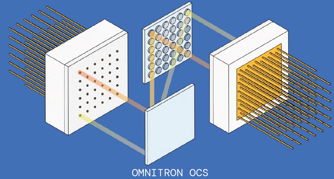
Omnitron OCS (Source: Omnitron Sensors)
In fact, since they don’t need illuminators or cameras, Eric says Omnitron’s technology could be used to implement a 1,200 x 1,200-channel OCS the size of a single Rubik’s cube.
In a crunchy nutshell, Eric says, “What we’ve developed is a mirror that has 10 times more force, 2 times more articulation, in-situ feedback and backside contacts, and simplified assembly boosting yield. What this adds up to is more channels for the data center, greater stability, lower loss, and real scalability. In short, we solved all four of the challenges stated by Google.”
Omnitron isn’t trying to out-Cisco Cisco. Instead, it’s supplying the missing piece—the MEMS mirror technology—that allows optical circuit switches to finally live up to their promise. Rather than selling a finished optical switch, Omnitron provides the core MEMS mirror technology that enables a new generation of OCS devices that are denser, more stable, easier to manufacture, and capable of scaling far beyond today’s designs.
Suffice it to say that if you’re wrestling with optical switching at the data-center scale, then Omnitron is a company that’s well worth a closer look.


Max,
A Nvidia H200 needs 600W to run, and a further 400W to circulate its coolant.
That is more energy input than an average European house.
We are literally turning hydrocarbons into teraflops, or petaflops or whatever.
What do these teraflops do for us?
Well Trump is going to get rich on cyber currency and Musk is going to get rich on providing AI for paedofiles.
Which bit of this are you happy with?
Personally, I’m not happy with any of it — but I’m all for cutting power consumption by 40% 🙂