


Smaller packages are always better, right? And you can’t get smaller than the die itself, right? I mean, if you can attach a bare die directly onto a substrate of some sort, then you’re not dealing with any space overhead caused by a package. Techniques for doing this are referred to – unsurprisingly – as chip-scale packaging, or CSP, indicating that the final packaged product is roughly the size of the chip itself.
Of course, when we talk size, we’re usually talking about the area of the die. But what about the thickness?
How Thin Can You Go?
Well, for the sake of structural integrity, you can go only so thin, right? Or else your die runs the risk of breaking or bending or something else that might put the circuits at risk. Breaking is obviously not a good thing, but what about bending?
We actually looked at that a few years ago in a piece covering some work done by the Korea Advanced Institute of Science and Technology (KAIST). The critical thing there was thinning a wafer and then transferring it to a flexible plastic substrate. And the critical question was, can the silicon survive the bending that happens on that substrate? Or, more precisely put, can the circuits survive?
The answer then was, “Yes,” but, at the time, it was a science experiment. Today, it’s apparently no longer an experimental thing. It’s formally called flexible hybrid electronics, or FHE. It’s hybrid because it bridges the gap between more traditional flexible electronics, which rely entirely on polymers for creating circuits, and silicon. In a presentation at the MEMS and Sensors Executive Congress late October, American Semiconductor talked about their semiconductor-on-polymer (SoP).
But before we dive into the details, let’s get some context. Who needs this, anyway? There are a number of market drivers that want to be able to do something other than flat. For one thing, there’s some aesthetic appeal to smooth, curved surfaces. They can feel friendlier, more organic, less clunkily robotic.
Part of it is also that, because we’re not used to seeing it with electronics, such shaping appeals to consumers: it’s cool. Now… I’m always a bit cautious when “cool” is a main motivator, since it comes and goes with the wind. So you need more than just the cool factor. But, when there are other drivers in addition, having the cool vote certainly helps you to get out into the market.
More specifically, American Semi sees cell phones, labels and tags, molding and lamination, curved automotive panels, and overall flexible electronics as markets that could really benefit from curvy circuits.
Adding Plastic to Make it Thinner
But, back to the size question: one would assume that using a plastic substrate would add to the thickness of a chip. After all, you’ve taken a die and added more thickness, right?
Actually… not right. In fact, the whole point of the thickness of a die is that it be rigid and that it can handle being handled without chipping or bending. Which goes against the whole flexible thing.
So, if you want a flexible silicon, why not just thin it down far enough that it gets bendy? Yes, it may be counterintuitive that a stiff material like crystalline silicon can be made to bend elastically, but, consistent with that intuition, silicon is still a brittle material. So if you had nothing but a super-thin chip, it’s not likely to survive the abuse it’s going to take between fab and board assembly.
Putting it on one of those plastic substrates, on the other hand, can add some stability; put simply, the plastic holds it all together, transferring some of the stresses that might otherwise damage the chip. You can then directly attach the encased die onto what amounts to a flexible PWB.
The upshot of this is that you can create a much thinner unit once you envelop it in plastic (in this case, polyimide, or PI) than you can with a bare die. From a packaged-part point of view, with direct chip attachment to a board, using only the chip itself (not in plastic), you can get down to 75 μm thickness. The thickness possible using American Semi’s FleX-IC approach? One third of that thickness: 25 μm.
One of the benefits of their approach is the fact that each die is surrounded by PI – including the sidewalls. This swaddles the die in PI, keeping it protected. It might not sound like a huge deal, but, if you think about it, it’s obvious (more or less) how you might place PI on the front side of the wafer, and it’s well known how you can use handle wafers to grind down the backside and apply PI there as well. But what about those sidewalls? Do you have to dice up the wafer before you can encapsulate the edges?
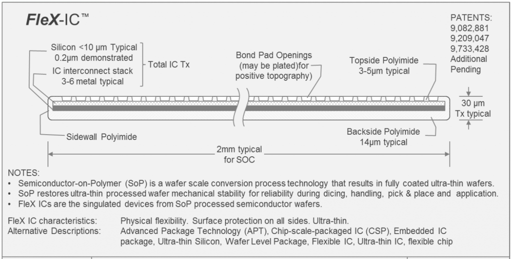
(Image courtesy American Semiconductor)
The answer is, “No,” but that’s about all we know; American Semi isn’t giving up its secrets. You’d think you could trench deep and… I don’t know, inlay PI somehow, but we’re talking the entire sidewall. So if you trenched before thinning, then thinning would effectively cut up the wafer once the grinder hit the depth of the trench. Of course, with PI in there, it might stick together at that point. But I’m simply speculating as I think through what the challenges could be; I don’t want to represent this as what they truly do.
Is it Reliable?
But how well does the plastic protect the die? That’s the focus of the reliability testing they’ve done and continue to do.
Their initial tests established the following results:
- They tested the radius of curvature (RoC): it passed at 1 mm. This is a much tighter bend than what KAIST did, where they could get breakage at 0.5 cm radius.
- A dynamic RoC test passed with more than 10,000 bend cycles.
- A torsion (or twisting) test yielded over 90,000 180° cycles.
- Testing metal de-layering passed for four-layer-metal CMOS.
- High- and low-temp operating life passed 168 hours at 125 and -25 °C.
- ESD passed at 4 kV (human-body model)
- Memory data retention passed 500 hours at 150 °C.
Next steps will test moisture sensitivity levels, thermal cycling, and highly accelerated stress tests.
They also demonstrated direct interconnect to flexible substrates using both a Z-axis adhesive and low-temp solder.
They’re preparing for market release of this technology as applied to dice of 100 leads or less. Going forward, they’re also in development on solutions for higher pin counts. This type of packaging has typically been limited to low-pin-count devices, but they’re saying that that should no longer be a limitation. That said, it remains ongoing work.
More info:


What do you think of flexible hybrid electronics and American Semiconductors’ approach to it?