


It’s the computer equivalent of the proverb, “If the mountain will not come to Muhammad, then Muhammad must go to the mountain.” If the data won’t come to your processor fast enough, send the processor out into the data.
That’s the idea behind GSI Technology’s first processor, called Gemini-1. It’s part memory chip, part processor chip, and all strange. But it’s also good at what it does, accelerating some specific mathematical functions by a whopping 100× compared to “normal” processors like an x86 or a GPU. Gemini-1 may not be for everyone, but nothing worthwhile ever is.
GSI may be new to the processor business, but the company has been around for over 25 years and employs more than 170 people. They’ve spent all that time making SRAMs, including some for military and aerospace applications. Even today, SRAM accounts for 100% of their revenue, according to Didier Lasserre, the company’s Vice President of Sales & Investor Relations. This whole processing thing is new to them.
Which may explain why they took such an… unorthodox approach with Gemini-1. It’s not another CISC, RISC, or even a VLIW machine. It’s more like an intelligent RAM, with millions of processing units scattered amongst the memory cells. With just the right software, dataset, and tailwinds, Gemini-1 can generate over 100 trillion operations per second. That’s a huge boost over even the most ambitious chips from Intel, Google, Nvidia, or GraphCore.
But it’s also highly specialized and not particularly suitable for most workloads. Can it play Flight Simulator? Run Linux? Boot an RTOS? No, no, and no. It’s basically a bitwise comparison accelerator, and GSI describes it as an APU: an associative processing unit.
Gemini-1 starts out as a large SRAM, which isn’t surprising given the company’s history. As with most SRAMs, the memory cells are arranged in nice, neat rows and columns, and – this is the important part – those rows and columns share read/write bit lines. GSI places a processor at the end of each bit line, where it can absorb the data coming from one or more SRAM cells in that column. Multiply that by the number of columns in the device, and Gemini-1 has about 2 million processing elements in total.
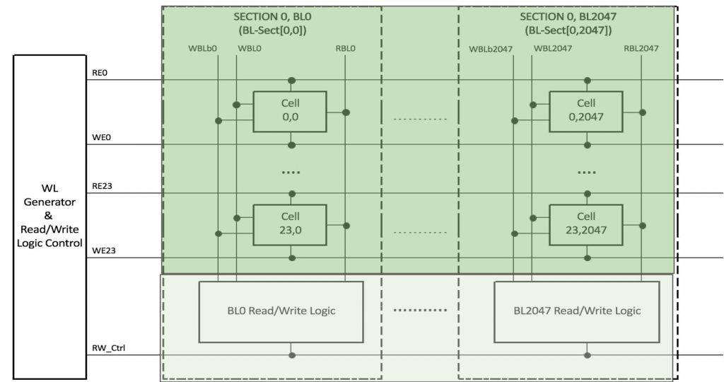
But Gemini’s many processors are simple – really simple. They can do a bitwise AND, OR, XOR, and invert, but that’s about it. Theoretically, that’s enough to create a “Turing complete” computer that could run any arbitrary code in the world, but that’s not really Gemini’s purpose. Instead, it’s geared toward massively parallel arithmetic/logic problems like you’d see in the inner loops of search or cryptography algorithms.
Specifically, Gemini is good at calculating Hamming distance, Tanimoto similarity, k-nearest neighbors (KNN), or SHA hashing functions. That makes it good at searching large databases of photographs or biochemical “fingerprints.”
The die photograph of Gemini-1 looks like any other SRAM, because it mostly is. The logic portion is vanishingly small. It doesn’t work like an SRAM, however. It’s partitioned into a 96-Mbit L1 cache, a 2-Mbit L2 cache, and a 48-Mbit area that GSI calls the MMB (main memory block). Whereas GSI’s commodity SRAMs are fabricated using 6T SRAM cells, Gemini uses a lot of 10T cells. The part is fabricated on TSMC’s 28nm process.
Programming Gemini-1 is as peculiar as its hardware architecture, but GSI is working to fix that. The entire chip – all 2 million processing units – will typically carry out the same operation, making Gemini-1 a massive SIMD machine. However, you can split the device in two, logically speaking, and have the two halves do different things. You can also divide it four ways, but that’s the limit.
GSI has some software libraries already in place, and more on the way, to make programming the chip more accessible. As it stands, coders need a bit of training from GSI, as well as a deep understanding of the chip’s design and of their own data. Sluicing data through Gemini-1 at top speed requires a careful look at how your data is partitioned and how it gets into and out of the device. Location is everything.
It’s one of the paradoxes of our age that memory is so much slower than microprocessors. That’s why we patch over the difference with caches, and caches on top of caches, seemingly ad infinitum. Moving data to and fro between CPU and RAM is a big waste of time and energy. That’s why GSI puts the processors where the data is.
But it’s far from the only company to discover this problem or to design a fix for it. Silicon Valley is littered with the carcasses of “intelligent RAM” companies that tried the processor-in-memory trick. They all failed, either because their chips were too hard to program, or because there weren’t enough real-world problems for them to solve. Part of the challenge is fabrication. Memory cells and logic gates don’t follow the same manufacturing processes, so one or the other (or both) get compromised. Advances in fabrication mean even bigger memory arrays and even more processing elements, which makes programming trickier, organizing data more difficult, and practical use cases harder to find. There are only so many problems you can solve by performing thousands of the same operation at once.
Still, GSI has discovered that if you’re extremely selective about your performance benchmarks, Gemini can outperform other processors by a factor of 100. It won’t be the main processor in your system, but it can make a remarkable accelerator given the right job.


This is interesting, but the concept ha been around for a very long time. When I was just starting in the early 70’s Signetics had this http://kazojc.com/elementy_czynne/IC/8220-4.pdf