


Ates Berna, General Manager and Managing Partner for ElectraIC in Istanbul, Turkey, recently posted a summary comparison chart showing the differences between FPGAs and ASICs on LinkedIn. Although it’s not a detailed chart, I think it’s a great icebreaker that leads to a more detailed discussion about the choices you make between an FPGA and an ASIC when you need a fairly complex high-performance, non-standard IC to solve a design challenge. (Note: The way Berna posted and tagged this chart on LinkedIn, I suspect it may have originated with Doulos, a training organization specializing in FPGA and ASIC design education. The chart compares FPGAs with “dedicated ICs,” which are clearly ASICs in this context.)
I have gotten the FPGA-vs-ASIC question frequently enough that I think there’s value in discussing the chart Berna posted. So here’s a more detailed, line-by-line discussion of the items in the chart:
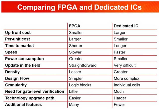
Here’s my line-by-line discussion of this chart:
Up-front cost: ASICs have large up-front costs. First, there’s the cost of the ASIC development tools. You need a fairly large tool chain to develop an ASIC, which you must either rent or buy, and you need to know how to use these tools. If your design team doesn’t have that knowledge, you’ll need to include the cost of training your team in your up-front cost list. In addition, you’ll incur a fairly large NRE (non-recurring engineering) charge, on the order of hundreds of thousands or millions of dollars, which you will pay to the silicon foundry to build your ASIC. The NRE charge pays for mask making and checking, reserving a slot in the foundry’s busy manufacturing schedule to make your ASICs, die testing and sorting, packaging, and final testing. By contrast, FPGAs are off-the-shelf parts, so there’s no foundry NRE charge, and FPGA tools are significantly less expensive than ASIC design tools, by perhaps three orders of magnitude. Depending on the FPGA, you can even purchase parts through distribution and get them the next day.
Per-unit cost: Here is where ASICs shine. Because you generally design an ASIC to meet your exact design requirements, you are buying only silicon you actually want. There’s little or no waste. So, assuming you have the projected product sales volumes to justify creating the ASIC, the ASIC should have a lower unit cost than an FPGA. That’s because FPGAs have significant silicon overhead. First, your design likely cannot use 100% of any given FPGA. If you’re lucky, you might get 90% utilization. Frequently, you may be unable to use as much as 10% or more of the FPGA’s resources to meet routability and timing goals because the routing congestion gets too great, and signals get too long and slow if you try to use the entire FPGA. In addition, signal-routing matrices on an FPGA are plentiful, to make sure you can route your design on the FPGA. As a result, the FPGA’s route utilization will be significantly lower than 90%, because you’ll never use all of the FPGA’s routing resources – everything can’t be connected to everything in a real design – but you pay for that FPGA routing silicon whether or not you use it.
Time to market: FPGAs are the time-to-market leader, by far. It’s possible to ship loaded boards on the same day that the FPGA design is finished, if you have manufactured pcbs at the ready. All you need to do is flash the final configuration into the EEPROM on the board, test it, pack it, and ship it. Conversely, when you finish an ASIC design, you ship the design to the silicon foundry and hold a tape-out party. Then, you wait several months while the foundry takes your design, checks it, manufactures the silicon, tests the die, packages the die, and then ships your packaged ASIC back to you. When you receive the finished box of ASICs, you can then build and test your boards. Meanwhile, a similar product from a competitor, but based on an FPGA, will have been selling in your market during those months that you were waiting to get your ASICs back from the foundry. If time to market is critical for you, FPGAs are probably the way to go.
Speed: ASICs extract the most performance from any given IC process node, assuming your designers know what they’re doing. FPGAs, thanks to their large (capacitive), programmable routing matrices, lose about an order of magnitude worth of performance from any given IC process node, relative to an ASIC’s performance.
Power consumption: It’s not obvious, but the same silicon inefficiency that FPGAs have relative to unit cost and speed also increase an FPGA’s power consumption relative to an ASIC. All of those extra routing-matrix transistors on an FPGA leak, contributing to higher static power consumption. The inherently longer routes in an FPGA, thanks to the Manhattan routing required in the orderly FPGA, add capacitance to every route, contributing to higher dynamic power consumption. However, it’s possible for FPGA vendors to fight back against the additional power consumption in their FPGAs. For example, Lattice Semiconductor has chosen a 28nm FDSOI process technology for its Nexus FPGAs to lower static power consumption. There are many such design tricks to lower power consumption, but FPGAs have large dies and large dies have a lot of capacitance, and they leak static power.
Update in the field: This is an easy one to understand. SRAM-based FPGAs are easily reprogrammed in the field. Change the configuration stored in flash memory and you update your design. In the early days of FPGA design, you had to pull the old configuration EPROM or EEPROM from its IC socket and plug in a new one to perform a field update. These days, you’re just as likely to design in reprogrammability through a USB or JTAG port. Some end-product designs permit wireless updates, although there are many security issues with allowing over-the-air hardware updates. Conversely, updating an ASIC generally requires a board swap (called a truck roll in the wireless industry). Some ASIC designs incorporate embedded FPGA (eFPGA) fabric from an eFPGA vendor like Achronix, Flex Logix, Menta, or QuickLogic to enable a limited amount of field updating without a truck roll. You can even get an open-source FPGA fabric generator and tool set called OpenFPGA if you want to take this approach. But if you embed an FPGA fabric in an ASIC, the ASIC becomes an FPGA, doesn’t it?
Density: Because device density is closely intertwined with unit cost, the same FPGA-vs-ASIC arguments apply, with one addition. In any given process technology, you can always design a bigger device, one with more resources, as an ASIC, thanks to the routing overhead and resource-utilization limitations of the FPGA, as discussed above.
Design flow: Unlike an ASIC, the FPGA’s physical design has been done for you and proven by the FPGA vendor before you ever see the device, errata notwithstanding. You will generally design an FPGA configuration using one vendor’s tool chain, although some well-heeled design houses employ ASIC-class place-and-route tools from one of the big-three EDA vendors: Cadence, Siemens/Mentor, and Synopsys. For ASIC design, you will generally take a mix-and-match approach, buying EDA tools from the big three and perhaps some additional design tools from newer EDA startups that haven’t yet managed to be absorbed by one of the big three EDA players.
Granularity: An ASIC’s digital granularity is one gate or, in some cases, one transistor. FPGAs must have much coarser granularity, on the order of one logic cell. Otherwise, the FPGA’s routing overhead would become completely impractical. This granularity difference between ASICs and FPGAs contributes to the FPGA’s higher unit cost and relative lack of density.
Need for gate-level verification: FPGAs require design-level verification just like ASICs. However, FPGAs are not granular at the gate level, so they don’t require gate-level verification. You place every gate in an ASIC design, so you need to verify each one.
Technology upgrade path: In theory, it’s easier to go from one FPGA family to the next within one FPGA vendor’s product line. For example, it’s relatively easy to migrate a design through the three Xilinx 7-series devices: Artix, Kintex, and Virtex. However, migrating to another vendor’s FPGAs means migrating to the other FPGA vendor’s design tools as well, and that’s not particularly easy, although it’s not as difficult as some people might have you believe. Engineers have managed to master more than one FPGA vendor’s tool chain. They just complain a lot while they’re making the change. There is no technology upgrade path for ASICs. To upgrade an ASIC, you need to design, verify, and manufacture a new one.
Additional features: Here, I must differ with the chart above. Although FPGA vendors have a long history of looking for additional functional blocks to add to their FPGAs, nearly anything available on an FPGA can be either designed or purchased as IP and placed on an ASIC. It might not be easy, but it’s generally possible. That statement about ASIC IP includes embedded FPGA IP. Perhaps the chart intends to suggest that it’s easier to take advantage of the many additional leading-edge features that FPGA vendors cram into their parts. For example, FPGA vendors have led high-speed SerDes design for the past 20 years. If you want a fast SerDes, you’ll likely find the fastest available on the newest devices from FPGA vendors, particularly Achronix, Intel, and Xilinx.
There are certainly many other design considerations that do not appear on the above chart. For example, there’s an intermediate step between FPGAs and ASICs – the structured ASIC – which offers many, but not all, of the benefits of an ASIC at a lower NRE cost compared to an ASIC. Fifteen years ago, many companies offered structured ASICs and suggested they were next-generation gate arrays. For many business reasons, there’s only one commercial structured ASIC vendor remaining – Intel – which bought the last remaining structured ASIC vendor, eASIC, in 2018.
Although the chart that triggered this article is not comprehensive, it does provide a good starting point when deciding between FPGAs and ASICs. By now, this article should have gored someone’s ox, so please feel free to leave a comment and let us know what you think.


2 thoughts on “FPGAs vs ASICs: Choose Your Path Carefully”