


When you spend a goodly chunk of your career dealing with EDA-like issues, as did I, then you have a pretty easy gut reaction to anything involving synthesis. See some kind of synthesis with a fancy new name? Must be some new crazy approach to generating logic circuits, right? Probably involving AI (which everything must have these days)?
Um… no. Today’s topic is sequential infiltration synthesis, or SIS. And, no, it has nothing to do with EDA. This happens in the fab. The fact that the story came from Imec for presentation at SPIE Advanced Litho should have been a clue. I was just slow to let go of my first reaction. So, if you also have some EDA in your past, then let’s step way back, cleanse our mental palate, and start again.
SIS is a process for hardening polymer films. Its semiconductor origins are with directed self-assembly (DSA), which uses two mutually repellant block copolymers. Their desire to keep a distance from each other allows features like dots and lines to appear naturally, as if by magic. But the materials also have a softness, and SIS was used to stiffen them up.
Through a process akin to atomic-layer deposition (ALD), SIS permeates the polymer with a metal oxide – in our case, aluminum oxide (also called alumina). That helps to give backbone to the softer polymer chains so that they retain their shape more readily.
So, outside of DSA, where else do we use polymer films that need to maintain strict pattern fidelity? Yes, photoresist. Imec did a paper for SPIE Advanced Litho on a project they took on to evaluate SIS benefits on photoresist – in particular, for designs employing extreme-UV (EUV) as the illumination source.
SIS for EUV
The motivation for this? In a word, “stochastics.” As noted in my recent SPIE overview, this is a hot topic these days, covering a number of the ills plaguing our ability to create ever-smaller features on silicon. In the Imec paper, they put a particular perspective on one of the challenges of EUV patterning: a paltry supply of photons. So, during exposure, you literally get spotty coverage.
I always thought of this as a simple result of the challenge of getting EUV power to the levels needed for high-volume manufacturing: those photons are hard to create, and we should be happy for the few that we get and make the best of it.
But there’s another, more fundamental, way to look at this. Each photon carries an energy related to its wavelength. EUV photons have way more energy than the photons we use for 193i lithography – as Imec tells it, 14 times the energy. So, if you measure your exposure dose in terms of the energy, then, for an equivalent dose, EUV will cut the number of photons by a factor of 14 as compared to 193i. Kind of obvious when you think of it that way, but, then again, you have to think of it that way.
So this statistical game results in a number of challenges, and Imec picked 4 metrics to determine whether SIS was useful as a lithography step. Those four metrics are:
- Line roughness. This has four different variants: roughness in the line edge (LER), line width (LWR), space width (SWR), and pattern placement (PPR). These are illustrated below, showing, from left to right, LWR, SWR, LER, and PPR.
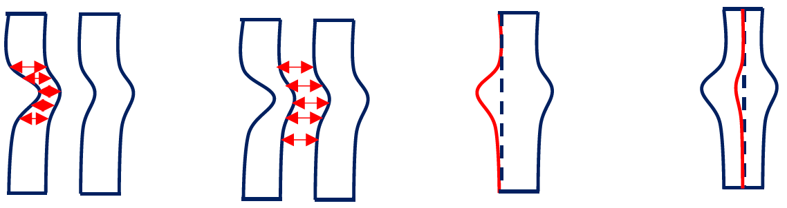
(Image credit Imec, SPIE; full citation below)
- Stochastic “nano-failures”: nano-bridges and nano-breaks between and in lines, respectively.
- CD uniformity, which is affected by shadowing on the reflective reticles (since it’s a multi-layer reflection thing, not just reflection off the surface)
- Tip-to-tip (T2T) CD uniformity. They focused on this in particular because, at small pitches, line ends tend to pull back.
There’s an additional consideration for this process: an underlayer that may be placed below the photoresist. Such underlayers, if chosen strategically, can help to amplify the sensitivity of the photoresist itself, further capturing and making use of as many photons as possible. But SIS is about infiltrating only the resist, nothing underneath. It turns out that many of the organic underlayer choices will themselves be infiltrated, making them unsuitable. So, in their experiments, Imec used spin-on glass (SOG) as the underlayer.
The SIS Process
So, with those issues as background, let’s talk about how this works. An ALD tool is used, with, in this case, tri-methyl aluminum (TMA) as the precursor. A conformal layer is deposited, and, through an infiltration mechanism that isn’t completely understood, the resulting aluminum oxide can migrate into the resist. This process can be repeated, and, by monkeying with the process, you can concentrate just a crust on the outside of the resist, or you can fully permeate the resist. In the latter case, you could even remove the resist afterwards, leaving only the aluminum oxide scaffold.
The specific stack they used involved lithography above an oxide/titanium nitride (TiN)/oxide sandwich, with amorphous carbon (a-C) as a hardmask and then layering on SOG and a standard chemically amplified resist (CAR). (It’s interesting that this process places metal oxide inside a CAR, even as metal oxide-based resists are evaluated as a competitor or successor to CARs.)
The process steps, illustrated below, involve:
- EUV exposure and development. The lavender features represent the pre-infiltrated, developed resist.
- SIS. The green features indicated infiltrated resist.
- Etching away the SOG and a-C.
- Stripping the infiltrated resist. Note that the resist strip must be able to take away the metal portion as well. They used an ammonia-peroxide mixture (APM).
- Pattern transfer down into the TiN.
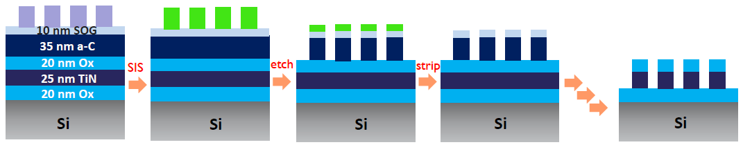
(Image credit Imec, SPIE; full citation below)
The SIS Results
And, referring you to the paper (below) for the gory experimental details and analysis, what did they get for their efforts?
- Roughness was reduced by 20% after lithography. Some of that was lost in the pattern transfer, reducing the improvement to 10% in the TiN. They recommend an optimized wet etch to preserve the smoothing that SIS provides before transfer.
- The number of line breaks was reduced by one to two orders of magnitude (depending on whether optical or SEM inspection was used). This translates directly into improved yield.
- CD uniformity within an exposure field was improved by 20% between two measurements: after lithography and after pattern transfer. In other words, uniformity actually improved after transfer. As compared to a reference process without SIS, the improvement was 60%.
- For a given local CD uniformity (LCDU), you can print a 20%-smaller T2T gap.
The cost of adding SIS to a process depends to some extent on whether you already have an ALD machine. If you do, and if you have availability to add SIS to its duties, then there’s an obvious cost advantage over having to buy a machine. That said, Imec says that it’s possible that the improved yield may pay for the extra cost and work.
More info:
Pieter Vanelderen et al, “Impact of Sequential Infiltration Synthesis (SIS) on roughness and stochastic nano-failures for EUVL patterning”, Proc. SPIE 10957, Extreme Ultraviolet (EUV) Lithography X, 109570S (26 March 2019); doi: 10.1117/12.2515503; https://doi.org/10.1117/12.2515503.
Sourcing credit:
Dr. Geert Vandenberghe, Sr. Manager, Exploratory Patterning Materials, Imec


What do you think of SIS as a way of improving pattern fidelity with EUV?