

We’ve reviewed a lot of sensors this year, both earlier and more recently, but there are a couple of other ones that need a few more column inches to describe. So today we look at new approaches to two unrelated sensors.
Finding Fingerprints
Our first story comes from Leti. They’ve announced a proof of concept for a new fingerprint sensor that has double the resolution of current standard versions. Today, folks deal with 500-dpi sensors, per FBI requirements; the Leti project yielded 1000 dpi. And they say that they should be able to drive that to 5000 dpi.
Because this is a proof of concept, their focus was entirely on the details of the sensor itself, not the supporting circuitry. So they didn’t design an accompanying ASIC. In fact, if this were to be commercially produced, a monolithic implementation – sensor and ASIC on one chip – would be best.
As it is, each pixel needs a wire – which is feasible on silicon, but would have to be part of that monolithic integration. Since they don’t have that yet, they had to limit the size of the array to 256 pixels because they were using external wiring. Clearly a motivator for integration, since then all of the wires would be on the metal layer, with no required inter-die interconnect.
They built the sensor’s transducer out of a piezoelectric material, ZnO, coaxing it to grow in bundles of vertical bristles. Each bundle is a pixel and is attached to a wire. The piezoelectric effect measures how much deformation occurs on each bundle; the analog signal is delivered via the wire. The choice of ZnO makes the sensor inexpensive, bio-compatible, and fab-friendly.
But, apparently, it’s not so easy to plant a forest of well-behaved PZ bundles. The key lies in the seed layer; they had to run many experiments to optimize the recipe for that layer so that it would encourage clean, vertical growth. Crystal orientation also matters, although the seed layer can help to compensate, since, in a monolithic integration with ASIC circuitry, other considerations might drive a different orientation.
Bundle location is determined by depositing a film of the seed layer material and then etching it away, except where the bundles will be grown. The image below shows a top view of a portion of the bundle array.
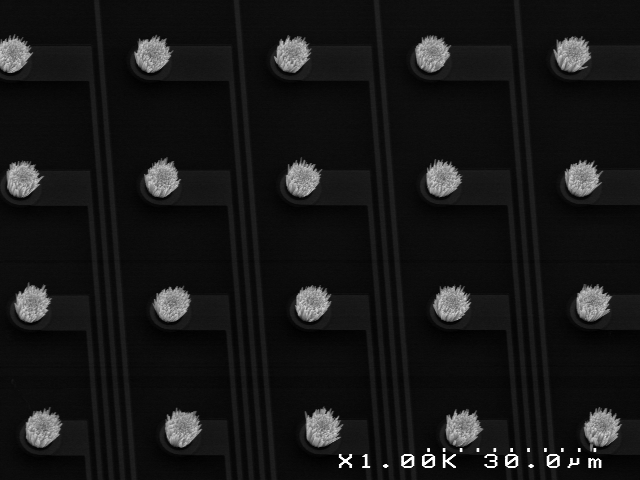
(Image courtesy Leti)
Figure 1. Fingerprint sensor pixels viewed top-down.
So what’s next? Well, that’s something of a “show-me-the-money” question. With proof of concept in place, the next steps will depend on partners being interested in investing in further developments Those efforts would further optimize the seed-layer recipe and integrate ASIC functionality onto the chip.
Longer Photon Travel
Meanwhile, OmniVision has announced a more sensitive night-vision sensor that detects near-infrared light; they call it their Nyxel technology. The benefit of that particular part of the light spectrum is that you can illuminate the field with infrared light to get a better image without a human being able to detect that the illumination is happening.
Their work focuses on the notion of quantum efficiency (QE). When light enters silicon, some of the photons create electron/hole pairs that can then be measured. Nothing new about this. The quantum efficiency is the number of electrons “liberated” for a given amount of light.
Problem is, much of the light enters the silicon and moves on through it without creating a measurable electron/hole pair. You can improve your lot by making the photons travel a longer path within the region you can measure. One way of doing that – which has been done already – is to increase the depth of the epitaxial layer where all this business takes place. The challenge there is that the electrons created lower down tend not to be particularly obedient about remaining beneath the pixel through which the light that created them entered. They may wander – effectively smearing the image.
![]()
(Image courtesy OmniVision)
Figure 2. Standard image sensor, with many photons escaping detection, reducing sensitivity – particularly a longer wavelengths.
Another way to create a longer path is to scatter the photons so they make a zig-zaggy path, increasing the distance they travel within a shallower layer. Even then, if you have a physical barrier to wandering electrons, then those electrons created deeper will remain confined to their neighborhood.
So OmniVision has created what they call a scattering layer on top, along with deep-trench isolation along the sides of the pixels. This makes for both a longer photon path and better-behaved electrons. Wondering how they did the scattering layer? Yeah, I was too. But you didn’t really expect them to divulge their secret sauce, now, did you? Yeah… they pled the 5th on that one.
![]()
(Image courtesy OmniVision)
Figure 3. OmniVision’s Nyxel technology, which employs a scattering layer, deeper epi, and deep trench isolation to increase low-light sensitivity, particularly in the near-infrared range.
Of course, as the QE charts show, response is for more than just infrared. If you’re using this in, say, a security camera, your point is to view the surroundings – day and night. The infrared portion realistically helps only at night. In fact, OmniVision says that including the IR signal during the day makes for a lower-quality visible image.
So higher-end cameras include an IR cut filter that can be mechanically placed in front of the lens. During the day, it remains in place to filter out the IR light. At night, it’s automatically retracted, allowing the IR signal. During the day, you have an RGB “full-color” image; at night, the RGB portion doesn’t receive enough light to matter, so you primarily get the IR light – emitted by the camera and reflected into the lens, yielding what looks like a black-and-white image.
By increasing the sensitivity through the Nyxel approach, they either get better visibility with lower illumination, saving power, or they can see further with the same illumination.
If you’re trying to include this in a camera of some sort, how easy that is depends on what you’re using now. If you’re already using an OmniVision sensor – one without the Nyxel technology – then they say that the new sensor will slide easily into the application. If you’re using someone else’s sensor, however, then it’s more of a redesign to incorporate this feature. No brand-agnostic plug-and-play interfaces here…
More info:


What do you think of Leti’s and OmniVisions sensors?