

“If I had to calculate 100% certainty on every deal I did, I would do zero deals.” – Chip Gaines
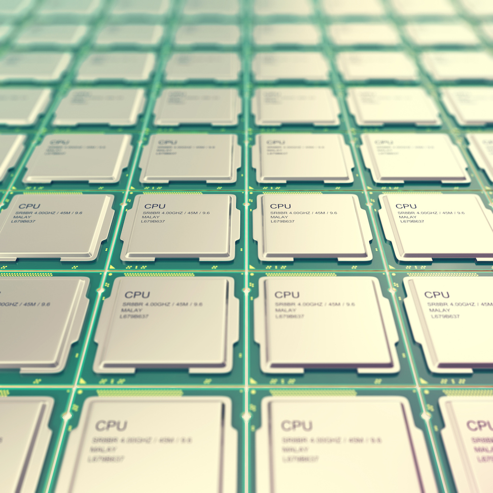
“Prodigy” is an appropriate name for the new microprocessor under development at Tachyum, a startup endeavoring to create “the world’s first universal processor.”
Their goals are nothing if not audacious. Prodigy will be faster than Intel’s Xeon but consume one-tenth the power. It will have 4× lower cost of ownership (TCO) than current server processors. It will occupy less silicon than an ARM design. It will perform both AI and hyperscale server workloads with equal aplomb. A single version of the chip will scale between 16 and 128 cores, all in the same 6400-ball package. And it will be cheaper than Intel or AMD chips by a factor of three. That last one shouldn’t be hard to achieve. The others? We’ll have to wait and see.
Tachyum employs about 55 full-timers and a number of contractors, split equally between two facilities in Santa Clara and Bratislava, Slovakia, which is also the home of the company’s founder, Radoslav Danilak. Microprocessor aficionados with long memories may remember “Rado” from his 1990s-era startup, DanSoft. Since then, Danilak has designed high-performance processors for a string of startups, including Gizmo Technology, Nishan Systems, Skyera, and others. He also did a four-year stint at nVidia. So, the man is no beginner when it comes to CPU architecture.
The Prodigy architecture combines a number of nonstandard architectural concepts. It’s a combination of RISC, CISC, and VLIW (very long instruction word) with multiple cores connected via an internal mesh network. It has its own instruction set but can also execute x86 binary code. And it prioritizes short wires to minimize routing and RC delays. “The problem is, transistors are connected by wires,” says Danilak, “and the wires are eating the benefit of the [faster] transistors.”
The initial version of Prodigy – one of four SKUs that will be based on the same silicon die and package – will boast 64 processor cores, arranged in an 8×8 grid. Later versions will have from 16 to 128 cores. Each CPU core is connected to its neighbors by synchronous links. Combined, these links make an on-chip mesh network that runs at the same 4-GHz frequency as the CPUs. There’s a one-cycle delay per “hop,” so communicating with an adjacent CPU is quicker than talking to one across the die. Thus, there’s some advantage to be had by partitioning workloads among neighboring CPU cores, a job Tachyum delegates to its compiler and linker.
Prodigy clusters its instructions together into bundles created by the compiler. A bundle may contain one to four 32-bit instructions, and each instruction can perform one, two, and in some cases three, operations. There are 32 integer registers (each 64 bits wide) and 32 vector registers (each 512 bits wide).
Instructions are dispatched across four integer units, three vector units, and three load/store units. The integer pipeline is 9 stages long, while the vector pipeline requires an additional five stages (14 total). Both are unusually short for such a complex machine. Most high-performance processors have 20-plus pipeline stages and struggle to reach 3 GHz.
Prodigy is able to handle data in a number of different integer and floating-point formats. Support includes the usual suspects, such as 8-, 16-, and 32-bit integers, the standard IEEE floating-point formats, and bfloat16. There’s also an unusual 8-bit floating-point format that’s unique to Tachyum and the Prodigy processor. It has just 3 bits of mantissa and 5 bits of exponent, which severely restricts its dynamic range but also reduces hardware requirements and allows Prodigy to handle multiple FP8 quantities at once using its existing registers and data paths.
Each Prodigy chip will also have from two to twelve DDR4/5 memory controllers, two Ethernet controllers, 16 to 64 PCIe lanes, and three levels of on-chip cache.
The L3 cache is a bit unusual. It’s physically divided up amongst the 64 CPU cores and acts either as a small private cache or as a larger shared “neighborhood” cache. In the former case, it’s a 512KB L3 cache that any CPU on the chip can read from, but that only the local CPU can update. In the latter case, it’s combined with the 15 neighboring L3 caches to make a shared cache that one-quarter of the CPUs can all use.
Prodigy will be bilingual, in the sense that it will run both its native instruction set (which has not been published publicly) and unmodified x86 binaries. Compatibility with x86 code is a must-have feature for any CPU intended to crack the lucrative server market. Amazon, Google, Microsoft Azure, and the rest have untold numbers of Xeon server racks, and that code isn’t going away soon.
Unlike, say, Transmeta, Centaur, or other x86 clones, Prodigy gets its x86 compatibility purely through software emulation, with no particular hardware assist. That ability comes courtesy of QEMU, the open-source emulation package. Danilak says Prodigy can run user-mode binaries at about 50% of native speed, based on his company’s simulations. That’s fast enough for most customers, he says, because it gets them up and running until such time as they convert and recompile their apps into native Prodigy code.
In native mode, Prodigy outperforms Intel’s best Xeon Platinum chips – in Tachyum’s simulations, anyway. The company has a “cycle approximate” simulator it uses for hardware and software development, and early results suggest better SPECint and SPECfp performance than its competitors’ published scores. Overall, Tachyum projects 10% or so better IPC (instructions per clock cycle) than x86. Combined with Prodigy’s higher core count and slightly faster clock frequency, the company expects great things from its offspring.
We may have to wait another year to know for sure, however. Prodigy is still on the drawing board, so to speak, although the preliminary netlist has passed EDA acceptance testing and the first layout of the chip is complete. So, it’s not obviously buggy. An FPGA prototype is expected in Q3 of this year, with tape out on New Year’s Eve, and samples in 1Q21. Assuming one minor metal-layer spin, production silicon could happen as early as 2Q21, or about 12 months from now. If all goes well.
That timeline puts Prodigy several months behind where the company said it would be 18 months ago. And the difficult, risky, and expensive parts of the project are still to come. It’s notoriously difficult to measure the performance of a complex processor on even the best of simulators, and even more speculative trying to estimate power. Price, at least, will be whatever Tachyum wants it to be.
The challenges are many. Any entirely new CPU architecture is likely to toss up entirely new bugs, bottlenecks, and unintended interactions. It also requires an entirely new and homegrown software toolchain. Even if Tachyum’s debut design is flawless, its aggressive 7nm fabrication and vertiginous target frequency can bring their own problems.
It’s unusual to have an on-chip network run at full CPU speed, especially when that speed is expected to hit 4 GHz. That’s an awful lot of tiny little 4-GHz antennas to wrap around your CPU logic. It’s also counterintuitive for a chip that’s supposed to consume 10× less power than Intel’s Xeon, which has far fewer CPU cores and no similar on-chip mesh network. Xeons have aggressive power and clock gating, which Intel euphemistically calls Turbo Boost. Danilak admits that Prodigy wasn’t designed with any power gating (it does have clock gating), making it hard to see where its power savings will come from. Tachyum must have a very efficient simulator.
Designing any new processor is a high-risk endeavor. But hey – no guts, no glory. Tachyum has set its sights high, and if the company achieves even half of its stated goals, Prodigy will be an impressive feat and a welcome new competitor in the high-end CPU market.


One thought on “Creating the Universal Processor”