

According to Greek mythology, the Chimera (a.k.a. Chimaera) was a monstrous fire-breathing hybrid creature that was composed of different animal parts. These days, the term “chimera” has come to describe (a) any mythical or fictional creature with parts taken from various animals, (b) anything composed of very disparate parts, or (c) anything perceived as wildly imaginative, implausible, or dazzling.
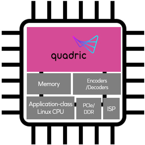
It is the latter meaning that is applicable to us here because I was just introduced to the Chimera GPNPU (general-purpose neural processor unit) from the clever chaps and chapesses at Quadric, and this little scamp certainly presses my “wildly imaginative” and “dazzling” hot buttons.
Founded in 2017, the folks at Quadric originally planned on providing inferencing edge silicon (i.e., chips targeted for inferencing applications at the IoT “edge,” which is where the internet meets the real world) based on their novel Chimera GPNPU architecture. Their first silicon was proven at speed, and some early adopter customers are already experimenting with it. More recently, however, those who don the undergarments of authority and stride the corridors of power at Quadric decided to license the Chimera GPNPU as IP that can be incorporated into other companies’ system-on-chip (SoC) designs, because this will expose their technology to a broader customer base.
In order to understand why the Chimera GPNPU is so “wildly imaginative” and “dazzling,” let’s start by considering the following image, which provides a simplified view of a facial recognition and authentication pipeline.
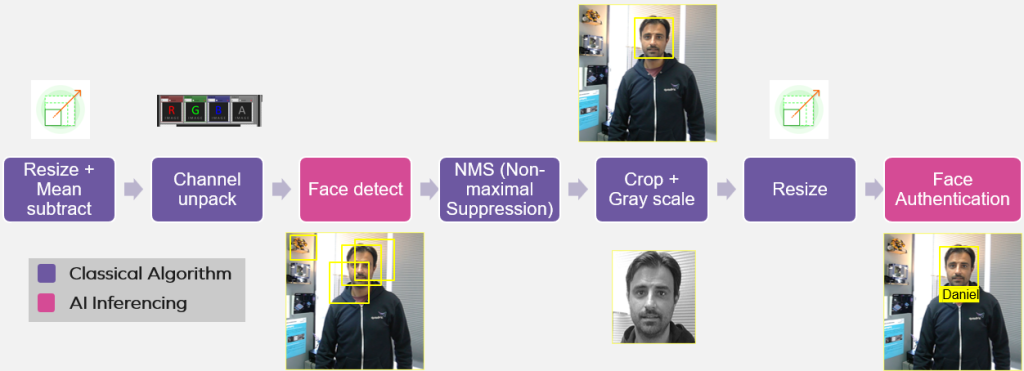
Facial recognition and authentication pipeline (Source: Quadric)
Let’s assume that all of these functions are implemented in a smart camera SoC. Let’s also assume that a camera/sensor is feeding a video stream into the first functional block on the left. This is something that we might expect to see in future generations of Ring Doorbell Cameras, for example.
Observe the two pink-colored “Face Detect” and “Face Authentication” functions, which are implemented using artificial intelligence/machine learning (AI/ML) inferencing. It’s amazing to think how rapidly the use of this type of inferencing has bloomed in the past few years, transitioning from an academic curiosity to early deployment to being almost a de facto element in modern software development.
The idea that employing inference (based on stimulus in the form of vision, sound, etc.) as just one of the building blocks developers use to create an application is something we might think of as “Software 2.0”; the problem is that it’s not as easy as I make it sound (everything can be made to sound easy if you talk loudly and gesticulate furiously). The way SoCs typically address the Software 2.0 challenge today is illustrated as (a) below.
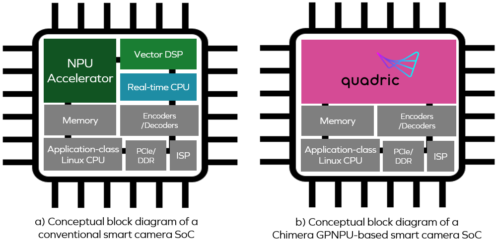
Conventional smart camera SoC vs. Chimera GPNPU-based SoC
(Source: Quadric)
The key point to note here is that the neural processor unit (NPU), vector digital signal processor (DSP), and real-time central processing unit (CPU) are presented as three separate cores. Now return to our facial recognition and authentication pipeline. Using the conventional approach, the processing associated with the first two blocks (“Resize” and “Channel Unpack”) would be performed on the DSP core.
The data generated by the DSP core would then be shuffled over to a neural network (NN) “Face Detect” graph/model running on the NPU core. The output from the NPU—a bunch of potential bounding boxes—would be shuffled over to the CPU core, which would run a “Non-Maximal Suppression (NMS)” algorithm to decide the best one to use.
The DSP would then use the bounding box identified by the CPU to perform more tasks on the image, such as “Crop + Gray Scale” and “Resize” (i.e., “Normalize,” in this case). Finally, this data would be shuffled over to an “Face Authenticate” graph/model running on the NPU core.
Suppose you implement things in this way, only to discover that you aren’t getting the frame rate/throughput you desire. How do you go about figuring out where the performance bottlenecks are? Also, how much power is being consumed shuffling data among the three cores?
The real underlying problem here is the fact that having three standalone processor cores makes the entire design process cumbersome. The hardware designers must decide how much memory needs to be assigned to each core and how big the buffers need to be between functional blocks, for example. Meanwhile, the software developers need to decide how to partition their algorithms between the cores. This is a pain because application programmers don’t want to spend a lot of time thinking about the hardware details of the target platform they are running on.
Another consideration is that ML models are evolving rapidly. Today, people are running visual transformers no one had even heard about a couple of years ago. Who knows what ML models will be running a couple of years in the future?
The fact that all of this is so horribly complex is one of reasons why deployment of ML hasn’t accelerated as fast as it could, because developing for this type of conventional target platform is a pain in the nether regions with respect to things like programing, debugging, and performance tuning.
All of which brings us back to the Chimera family of GPNPUs, which are represented by the pink area in the (b) portion of the previous illustration. The GPNPU combines the best attributes of DSPs, CPUs, and NPUs in a single core that acts as the combination of a conventional CPU/DSP that can run C/C++ code with a complete 32-bit scalar + vector instruction set architecture (ISA) along with an NN graph processor that can run ML code optimized for 8-bit inference. This approach uniquely solves the signal chain challenge by allowing developers to run both types of code on the same engine.
We might think of the Chimera GPNPU as being a hybrid between a classic von Neumann RISC machine and a systolic array/2D-matrix architecture. From the processor standpoint, we have single 64-bit instruction words coupled with a single-instruction issue/clock. We also have scalar and vector/matrix instructions modelessly intermixed from clock tick to clock tick.
One of the key advantages of the Chimera GPNPU approach is its ability to adapt to evolving and increasingly sophisticated ML networks. Things like transformers are getting to be more and more complex, wanting to do more conditional control flow within the architecture of the NN, be it a CNN, RNN, DNN, etc. Conventional NPUs are often like hard-wired accelerators that can’t perform conditional execution. For example, you can’t stop somewhere on layer 14 and check for conditions or intermediate results and then branch and do various control-flow-oriented things if you have a dedicated accelerator. In those cases, you have to shuffle data back and forth between the NPU and CPU, which results in hits to performance and power. By comparison, with a Chimera GPNPU, you can literally switch back and forth between the NN and your control code on a clock-by-clock basis.
There’s so much more to talk about here, such as the way the Chimera GPNPU excels at executing convolution layers, which are at the heart of CNNs, and their TOPS (trillion operations per second) scores, which bring tears of joy to my eyes. Unfortunately, this is a case of “so much to do, but so little time to do it all” (the folks at Quadric will be delighted to tell all if you give them a call).
The final topic I wanted to touch on here is to give a quick overview of the Quadric software development kit (SDK), as illustrated below.
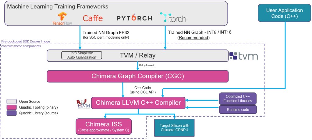
Quadric’s software development kit (SDK) (Source: Quadric)
The bottom line is that everything is driven by software. The trained NN graph/model generated using a framework like TensorFlow, PyTorch, Caffe, etc. is fed into Apache TVM (an open-source machine learning compiler framework for CPUs, GPUs, and ML accelerators) which generates a Relay output (Relay is a high-level intermediate representation of the TVM framework).
Conversion and optimization of the Relay representation is performed by the Chimera Graph Compiler (CGC), which outputs the transformed and optimized NN as C++ code. The Chimera LLVM C++ Compiler merges this code with the developers’ C++ application code, and the output from all this is an executable that runs on the Chimera GPNPU in the target silicon/SoC.
Observe that the Quadric SDK is delivered as a prepackaged Docker image that users can download and run on their own systems. Quadric will soon have this SDK hosted on Amazon Web Services (AWS), thereby allowing users to access it via their web browsers.
Of particular interest to me is that the folks at Quadric are working on a graphical user interface (GUI) that will let developers drag-and-drop pipeline building blocks containing CPU/DSP code and NPU graphs/models, stitch them together, and compile everything into a Chimera GPNPU image. This no-code development approach will empower large numbers of developers to create applications for silicon that has a Chimera GPNPU in it.
Phew! I’m really excited by all of this. I think the application areas for this sort of technology are limited only by our imaginations. What say you? Do you have any thoughts you’d care to share?


