


The phrase “wake up and smell the coffee” is an idiom that means: “Pay attention to what’s really going on.” It’s not that this is in any way relevant to the following discussions: I was just wondering where and how this expression originated.
Now I come to think about it, this query was sparked by my hearing the news that the folks at Xilinx (now part of AMD) are celebrating June 2025 as the 40th anniversary of the first time a physical field-programmable gate array (FPGA) bid a cheery “Howdy” to the world. (The reason for the “physical” qualifier is that although the first FPGA was “announced” in 1984, it didn’t physically manifest itself until 1985.)
In turn, this prompted me to dispatch the butler to retrieve my reflective trousers. By this, I don’t mean shiny metalized mylar leggings (“Not that there’s anything wrong with that,” as Jerry Seinfeld famously said). Instead, I’m postulating a pair of contemplative slacks that are comfortable and supportive of a reflective mood (I could waffle for the USA’s Olympic team if the games committee were to support such an event).
One concept that kicked off some cogitation is the consideration that we are so busy racing through life that we don’t take the time to slow down and reflect on how we’ve come so far so fast (or “How did it get so late so soon?” as Dr. Seuss would have it). Perhaps we should “Slow down to smell the silicon, “Pause to appreciate the pixels,” and “Take a moment to marvel at the magic,” as it were.
For example, my maternal grandmother was born in 1898, which was five years before the first successful airplane flight. My dear old dad was born in 1915, which was five years before the first commercial radio broadcast. And my sweet old mum was born in 1930, which was five years before the first voice-over TV broadcast by the BBC in the UK (this was also five years before the first canned beer was sold in the USA, but my mum doesn’t drink beer, so that’s not particularly relevant to these discussions).
Just to set the scene, when I started my career as a hardware logic design engineer at the beginning of the 1980s, most integrated circuits were “frozen in silicon.” The only programmable (customizable) logic devices (PLDs) available to us were simple PLDs (SPLDs) and complex PLDs (CPLDs).
SPLDs included PROMs (circa 1970), PLAs (circa 1975), PALs (circa the late 1970s), and GALs (circa the beginning of the 1980s). Early CPLDs, which started to arrive circa the tail-end of the 1970s, essentially consisted of several SPLDs sharing a common programmable interconnection matrix, all implemented on the same silicon die.
Although all these devices were limited in capacity and functionality, we certainly managed to manifest a myriad of uses for them. In the case of SPLDs, for example, we used them for “glue logic” (replacing multiple discrete 7400-series TTL gates with a single programmable device to reduce board complexity and power), address decoding, implementing small finite state machines (FSMs), bus interface logic, simple input/output (I/O) decoding, signal conditioning and timing adjustments, security and protection logic (e.g., adding simple access control or protection mechanisms to embedded systems), and… the list goes on. CPLDs extended the capabilities of SPLDs and were used in more demanding scenarios.
There were two great aspects to these PLDs. The first was that their timing was 100% deterministic (I recall data sheets specifying different delays from rising and falling edges on inputs to rising and falling edges on outputs). The second was that they spawned languages/tools like PALASM (PAL Assembler), ABEL (Advanced Boolean Expression Language), CUPL (Common Universal tool for Programmable Logic), and AMAZE (Automated Map and Zap of Equations). These tools and hardware design languages (HDLs), which were precursors to languages like Verilog and VHDL, allowed users to capture design intent and program the devices. It was like magic!
As an aside, if you want to learn more about all this stuff, I cover SPLDs and CPLDs in excruciating exhilarating detail in my books, Bebop to the Boolean Boogie and The Design Warrior’s Guide to FPGAs.
And then came the FPGA. This was the brainchild of the American electrical engineer and inventor Ross Freeman, who is widely recognized as being the father of FPGAs. Ross conceived the idea of a general-purpose programmable logic device that combined the flexibility of software with the speed of hardware. In 1984, along with Bernard Vonderschmitt and James Barnett, Ross founded Xilinx in Silicon Valley.
The first FPGA to see the light of day was the XC2064, which was implemented in CMOS at either the 3µm, 2.5µm, or 2µm process node, depending on who you are talking to. Containing ~85,000 transistors, the XC2064 boasted an 8 x 8 = 64 array of logic blocks “islands,” each containing two 3-input look-up tables (LUTs), all sitting in a “sea” of programmable interconnect fabric.
The number of pins depended on the package. For example, the XC2064-PD48C was presented in a 48-pin DIP (Dual In-line Package) package, as seen below.

XC2064-PD48C (Source: AMD/Xilinx)
AMD acquired Xilinx in 2022 (they announced their intention to do this in 2020). In many ways, this was a “match made in heaven,” but that’s a discussion for another day. I was just perusing and pondering the From Invention to AI Acceleration: Celebrating 40 Years of FPGA Innovation blog on AMD’s website. I love the picture of Ross looking at the XC2064 layout.
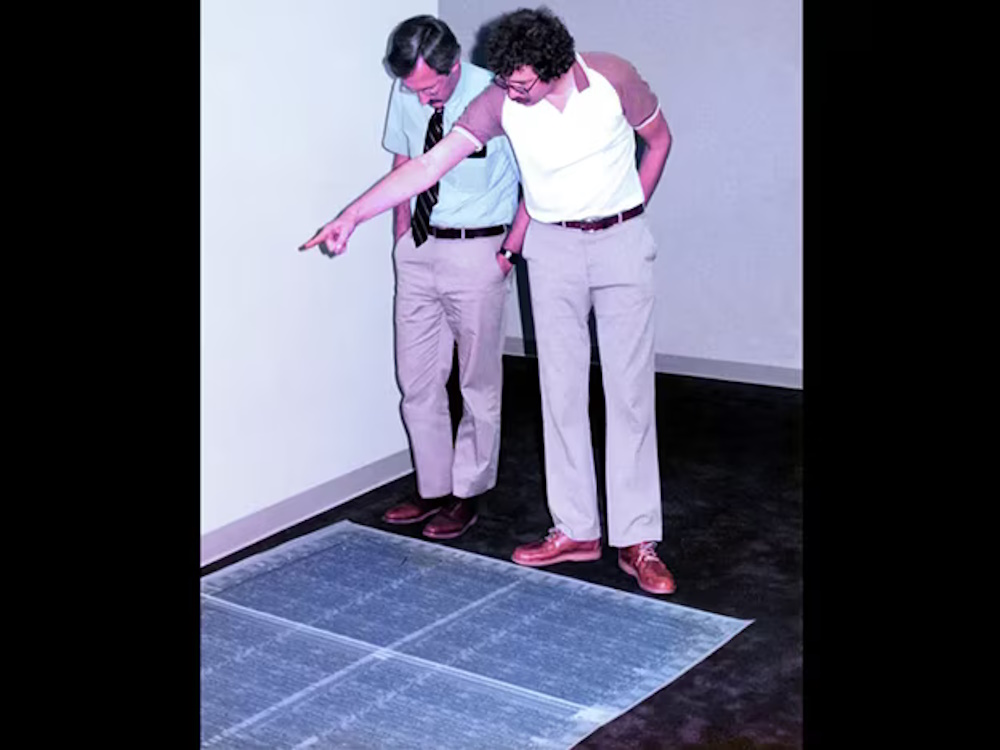
Ross Freeman (right) getting a bird’s-eye view of the XC2064 layout (Source: AMD/Xilinx)
I’d also love to learn who’s standing next to Ross, but no one I know seems to know. Sad to relate, Ross passed away in 1989, only a few years after creating a new industry and launching what was to become a multi-billion-dollar company.
One of the problems in the early days was the lack of good FPGA tools. I’m not an expert here, but I seem to remember hearing that users employed simple schematic capture to describe how the logic blocks and I/O blocks were to be connected inside the device. Also, the users had to specify the contents of the LUTs by hand. It wasn’t until circa 1990 that Xilinx introduced XACT, which either stood for Xilinx Automatic CAE Tools or Xilinx Advanced CAD Technology (it’s amazing how much has been forgotten in just a few decades). This encompassed place-and-route (P&R), static timing analysis (STA), and bitstream generation.
A big issue with pre-XACT design methodologies was the fact that it was almost impossible to determine a design’s input-to-output delays without actually programming a device and measuring its real-world timings. I remember thinking, “FPGAs are an interesting idea, but they’ll never catch on.” This provides just one more example of why I’m destined to die in poverty as a sad and broken man.
How the world has changed. Today’s high-end FPGA offerings can contain millions of LUTs and billions of transistors. In addition to thousands of DSPs, megabytes of block RAM, and gigabytes of in-package high-bandwidth memories (HBMs), they can also contain multiple processors (CPUs, GPUs, NPUs, etc.). In the case of FPGAs that contain processor cores along with their programmable fabric, these are typically referred to as System-on-Chip (SoC) FPGAs.
Another change that has taken place is the capacity and sophistication of the tools used to design these devices. My own simplistic view of the AMD/Xilinx SoC FPGA tool hierarchy is depicted below.

A hierarchical cornucopia of cunning tools (Source: Max Maxfield)
First, we have Vivado, which can be used on its own by traditional hardware developers who delight in working at a low level of abstraction called RTL (register transfer level) (When I say “low level,” I mean in the context of what’s “sitting on top” as discussed below. Everything’s relative, even my Auntie Barbara. The RTL supported by Vivado is “high level” compared to the way we used to design things when I started out.)
Next, we have Vitis HLS (high-level synthesis), which allows software developers to capture their design intent in C/C++/OpenCL. The output from Vitis HLS is RTL that feeds Vivado.
And for people designing artificial intelligence (AI) and machine learning (ML) systems, we have Vitis AI, which accepts AI frameworks like TensorFlow, PyTorch, and ONNX, and outputs the C/C++/OpenCL that feeds Vitis HLS.
And then things get complicated…
And then I get confused…
To be honest, I’m currently spending so much of my time running around in ever-decreasing circles shouting “Don’t Panic!” that this 40th anniversary may well have slipped past without my noticing. Fortunately, I was just chatting with Brian Garabedian, who is Senior Manager, Global Communications at AMD, and Kirk Saban, who is Corporate VP of Marketing for the Adaptive Embedded Computing Group at AMD (Kirk covers both FPGA and classic embedded X86 processor-based products).
Brian and Kirk told me that everyone at AMD/Xilinx is bouncing around with excitement with respect to this 40-year anniversary, which will be featured at this year’s Advancing AI event. By some strange quirk of fate, the Advancing AI extravaganza takes place on June 12, 2025, which is the same day this column made its debut on the EEJournal website (what are the odds?).
If I ever get my time machine working (you simply cannot find the spare parts where I live), two things I’ll add to my “To Do” list are (a) travel back to 1984 when Xilinx was founded and visit Ross to tell him what will become of his invention, and (b) buy as much Xilinx stock as I can lay my hands on.
What say you? Do you have any thoughts you’d care to share on any of this? In particular, if you worked with the original XC2064 FPGAs, I’d love to hear about the design tools and techniques you used.


