


A new sensor technology just popped up under my nose shouting “SURPRISE” (metaphorically speaking, of course). In this case, we’re talking about a technology that can take a traditional 2D CMOS camera sensor and use it to generate both 2D and 3D images. This was just when I thought I’d seen it all (no pun intended). Color me impressed!
“What is this incredible technology and who makes it?” I hear you cry. Don’t overexcite yourself. Settle down into your seat and I will reveal all. I was just chatting with my old friend Jean-Sébastien Landry, who is Director of Product Management at AIRY3D. This is a small, feisty company that’s invented an awesome way to extract a 3D depth map (a.k.a. 3D point cloud) using a standard 2D CMOS sensor. “Well, I certainly didn’t see that coming,” I thought to myself.
Before we plunge into the fray with gusto and abandon, let’s pause for a moment to think about the traditional techniques we can use to extract 3D information from a scene. Let’s start with the way we (humans) do things using our biological systems. Each of our eyes (left and right) receives a different image due to their slightly different positions in our heads. These positional differences are referred to as “horizontal disparities” or “binocular disparities,” and these disparities are processed in the visual cortex of our brains to yield depth perception.
In the case of machine vision, we can do much the same thing using two cameras, each equipped with a lens focusing the image onto a CMOS sensor. We can take the images from both sensors, perform a humongous amount of processing, and extract detailed 3D depth information from the scene.
Since our brains are so awesome (I can safely say mine is one of my top three favorite organs), we can also perceive depth using only one eye. If we are playing catch with a friend, for example, we can track and grab the ball out of the air, even with one eye closed. This is because our brains exploit all sorts of visual cues, such as the fact that we know what sizes we expect things to be, so if something whose size we know looks smaller, then we know it’s further away. If it starts to look bigger and bigger, then we know it’s time to duck. Our brains also understand things like perspective, where things like parallel lines (think railway tracks) get closer together the further away they are. And, if we are moving, there’s motion parallax whereby things appear to move at different rates depending on their distance from us.
Once again, we can use similar techniques in the case of machine vision. That is, we can take the images from a single CMOS sensor and use artificial intelligence (AI) to detect and recognize objects. Then, based on its knowledge of those objects, the AI can estimate the depths associated with different elements of the scene. The two big problems here are (a) the humongous amount of processing that’s required and (b) the fact that AIs can suffer from hallucinations (responses containing false or misleading results).
Like our eyes, the CMOS sensors we are talking about here are passive, which means they detect energy supplied from an external source (like the sun) and do not themselves generate any energy. By comparison, active sensors like LiDAR transmit energy and detect the signals returned when that energy bounces off something. Now, LiDARs are great, and it’s certainly true that they are falling in size, power consumption, and cost, but they are still huge, power-guzzling, and much more expensive as compared to a traditional CMOS sensor.
All of which brings us back to the guys and gals at AIRY3D and their unique DepthIQ technology for 3D vision. In a crunchy nutshell, these little scamps have developed a hardware-enabled solution that can extract 2D images and 3D depth maps simultaneously from a single passive CMOS sensor. Using DepthIQ, a 3D camera can be built at a fraction of the cost, size, power, and compute load as compared to a standard stereo camera.
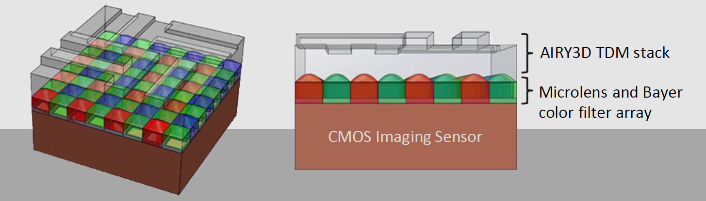
Are you just a tad skeptical? I know I was. Do you think this sounds too good to be true? I know I did. Then Jean-Sébastien tore the veils asunder causing me to squeal in delight (not out loud, but I was definitely squealing inside). The amazing thing is that—conceptually speaking—this is all so understandable, even for a bear of little brain like your humble narrator. The hardware portion is a transmissive diffraction mask (TDM) that’s applied on top of a standard CMOS sensor manufactured using standard CMOS processes.
DepthIQ is a hardware-enabled software solution (Source: AIRY3D)
Jean-Sébastien says that they’ve successfully implemented this TDM on sensors from multiple vendors. Now, this is where things start to get clever. As the light passes through the diffraction grating, it’s modulated before it lands on the underlying pixels, where this modulation encodes depth information.

DepthIQ takes advantage of the light itself (Source: AIRY3D)
The way to think about this is that we’re letting physics “do the math” with the diffraction performing most of the computation. Before we proceed, consider a traditional 2D image pipeline as illustrated below.

CMOS Sensor + Image Signal Processor = 2D Vision (Source: AIRY3D)
From left to right we have a lens assembly focusing light on a standard 2D CMOS sensor. The raw data from the sensor is fed to an image signal processor (ISP) that performs any computation required before passing the resulting 2D images to any downstream applications. The ISP algorithms can be implemented in software running on a processor or in hardware running in silicon.
Now take the same CMOS sensor but with a TDM applied as shown below. Once again, the raw data is passed to the image processing unit. This time, however, a pre-filtering decoder is used to decouple the regular image data, which is fed to the original ISP, and the modulated depth image information, which is fed to an image depth processor (IDP). As for the ISP algorithms, the IDP algorithms can be implemented in software running on a processor or in hardware running in silicon.

TDM + CMOS Sensor + Lightweight Algorithm = 3D Vision (Source: AIRY3D)
All this processing is hardware agnostic and can be performed on any processing platform—CPU, GPU, NPU, DSP, FPGA, ASIC/SoC, etc.
The result is a high real-time frame rate providing perfectly aligned 2D images with 3D depth maps without any additional processing required.
The applications for this technology are limited only by our imaginations but include things like automotive sensors (including in-cabin occupancy), industrial sensors, mobile sensors, robotics sensors… the list goes on. For example, this video shows some members of AIRY3D’s optics team taking a short road trip.
The left-hand side of the screen shows a regular black-and-white image, while the right-hand side reflects the frame-synched 3D depth map. The regular image could be passed to an AI, which could also make use of the associated depth information.
Another example that really caught my eye was a demonstration of a video conferencing application whose “background blur” algorithm has been augmented with 3D depth perception as shown below.
Funnily enough, this happened to me just the other day. I was on a video call with someone who was trying to show me something, but his system kept on blurring it out. Eventually, he turned the blur off, revealing a very untidy room (I could see why he wanted to use the blur filter).
I tell you… I can see so many applications for this sort of thing. And the important point to note here is that this isn’t all a “pie in the sky” theoretical prototype. The folks at AIRY3D are working with various partners on a variety of real-world products. For example, consider the recent announcement of the launch of Teledyne e2v’s Topaz5D featuring AIRY3D’s technology. This 1,920 x 1,080 resolution, low noise, global shutter 2D and 3D image sensor can be used to power many next-generation applications, from smart doorbells to industrial handheld scanners to automated mobile robots (AMRs).
All I can say is “O-M-Goodness gracious me. What will they come up with next?” But it’s not all about me (it should be, but it’s not). What do you think about all of this?


