


FPGA place-and-route software goes too fast, said no one ever. In fact, FPGA vendors have spent considerable effort in making their design software run faster on multicore processors. A paper recently presented at the ACM’s FPGA 2022 conference titled “RapidStream: Parallel Physical Implementation of FPGA HLS Designs,” describes a very interesting approach to pushing HLS designs through FPGA design software running on multicore processors faster. The paper – authored by a large team of researchers at UCLA, AMD-Xilinx, Ghent University, and Cornell University – describes RapidStream, which is an automated partitioning algorithm that slices up a dataflow design into multiple “islands,” inserts registered “anchor regions” between the partitioned islands, and then stitches up the entire design by routing signals from each island through the registers in the anchor regions.
The purpose behind all this partitioning and stitching is to chop up the HLS design into bite-sized chunks that can be handed off to the many cores in a modern server. It’s the age-old divide-and-conquer strategy used by engineers for centuries, now adopted to accelerate FPGA development.
This process has three main HLS-level constraints:
- Non-overlapping partitioning – To parallelize the physical implementations of different islands, each island must contain a unique and non-overlapping partition of the design.
- Pipelined inter-island connections – Each inter-island connection is pipelined to meet timing and achieve timing closure.
- Direct neighbor connections – Each island can have direct connections only with immediately adjacent islands. This constraint turns out to be critical when parallelizing design placement and routing.
(Note: These constraints are nothing like the various constraints you use to control logic synthesis. They’re at a higher level.)
RapidStream’s creators define a dataflow design as a collection of parallel processing elements (PEs) and a set of FIFOs that connect the PEs to each other as defined by the design’s dataflow needs. Each PE can be arbitrarily complex internally, but it must communicate data to other PEs only through FIFO interfaces. As mentioned above, RapidStream divides the FPGA fabric into two types of regions: equally sized islands and anchor regions placed in thin columns and rows between the adjacent islands. Interestingly, RapidStream seems to have been specifically built for AMD-Xilinx Virtex UltraScale+ FPGAs, which are 2.5D devices made with FPGA chiplets – Super Logic Regions or “SLRs” in AMD-Xilinx speak – bonded to a silicon substrate. Xilinx pioneered this construction technique for FPGAs and has been using it for several FPGA generations, for about a decade. The reason this fact is important is because there’s a natural partition between AMD-Xilinx SLRs, and RapidStream seems to have been written and its algorithms specifically designed to take this SLR physical partitioning into account, as the figure below, taken from the FPGA 22 paper, illustrates.
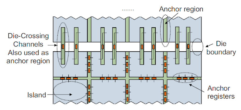
RapidStream partitions an HLS design into islands containing Processing Elements (PEs) and anchor regions that provide FIFO communications registers between communicating islands.
When you feed a dataflow design described in HLS to RapidStream, it partitions the design using the three-phase process:
Phase 1: Slice the HLS dataflow design into roughly equal partitions (or PEs) that will fit into the predefined islands. RapidStream takes advantage of the dataflow design’s elasticity to make certain that every inter-island (or inter-PE) connection is pipelined through an anchor register, which ensures that the partitioned design’s timing will provide the isolation required for parallel placement and routing.
Phase 2: Place and route the disjoint islands and insert the anchor registers. Rapidstream uses a simple distance-driven placement algorithm for this phase, which achieves similar timing quality compared to a standard FPGA placer, but it runs much faster. Further, each PE island can be placed and routed by a different processor core because they’ve been made independent of each other during partitioning. A clock management scheme ensures that the clock skew is consistent among the islands when they are routed and later stitched together. This step avoids hold violations after stitching.
Phase 3: Stitch the placed and routed islands together through the pre-placed anchor registers. Because of constraint 1 above, the inter-island connections are anchored, so the stitcher only needs to route each island to its surrounding anchors and then on to the adjacent island. This scheme greatly simplifies the stitching task, with the exception of the design’s global clock, which is a global net that fans out to all islands.
Of course, I’ve skimmed over a lot of the details. You can get those from the paper. The real question is, “How well does this idea work?” The answer: pretty well.
The paper contains a couple of charts that describe how well RapidStream works. The first chart shows the clock rates achieved by six different dataflow designs after partitioning compared to the pipelined and non-pipelined versions of the same design without partitioning.
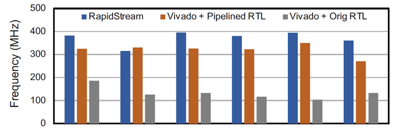
RapidStream partitioning improved the clock speed of five out of six RTL designs compared to a pipelined but non-partitioned design.
The RapidStream results are the blue bars, which show faster clock rates than all of the non-partitioned, non-pipelined versions of these designs. You’d expect that result. Pipelining is at the very core of clock-speed improvement in FPGA design. However, the RapidStream results are better than the pipelined RTL versions of the same design in five of the six cases. That result should really get your attention.
Next, here are the place-and-route timing results from the paper:
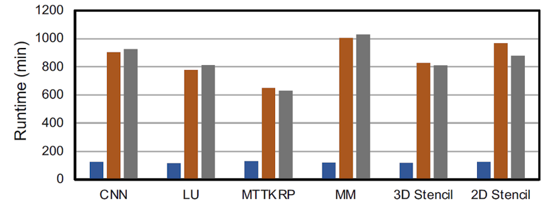
RapidStream improved place-and-route run times for six out of six RTL designs compared to a pipelined or non-pipelined, non-partitioned designs.
RapidStream’s place-and-route runtime results are much better than the results for the unpartitioned design. Again, that’s because RapidStream can hand each partition off to a different processor core for placement and routing. Although FPGA vendors have tried to make their place-and-route algorithms work faster with multicore processors, RapidStream’s developers empirically discovered that there’s not yet much benefit from more than about two processor cores (2.1 processor cores, more precisely) when running the AMD-Xilinx Vivado Design Suite of tools if the FPGA design isn’t partitioned.
By now, you should have your interest piqued by RapidStream if you’re developing HLS designs with FPGAs — particularly AMD-Xilinx FPGAs. You can find more information about the RapidStream project on its GitHub page.


With a Flowpro parallel computational machine all of the objects and tasks are already petitioned at the source level of the design. It seems that a true parallel substrate machine such as Flowpro could easily take advantage of multicore synthesis.