


Way back in the mists of time that we used to call 2023, I wrote (well, waffled) a column about Network-on-Chip (NoC) technology (see Who Needs a Network-on-Chip (NoC)? Everyone!). Suffice it to say that this was in the days before the punctuation police forbade me from using exclamation marks in my titles (thankfully, I’m not bitter).
Well, even though this was but two short years ago, all I can say is that NoC technology has progressed in leaps and bounds since then. Before we plunge headfirst into the fray with gusto and abandon (and, always, with aplomb), let’s briefly remind ourselves how we arrived at using NoCs in the first place.
Let’s start with the fact that a System-on-Chip (SoC) is an integrated circuit (IC) that incorporates all—or most—of the components of a complete computer or electronic system onto a single chip. This typically includes the following:
- Processor cores and hardware accelerators (e.g., CPUs, GPUs, NPUs, TPUs)
- Internal memory blocks and controllers (e.g., RAM, ROM, Flash)
- External memory controllers (e.g., DDR, NAND Flash)
- Input/Output interfaces (e.g., USB, HDMI, UART, SPI, DDR)
- Communication modules (e.g., Wi-Fi, Bluetooth)
- Power management circuits
- Mixed-signal components (e.g., ADCs, DACs)
- Peripherals (e.g., timers, controllers)
Just to keep things simple, let’s assume that all these functions start off as intellectual property (IP) blocks specified at the register transfer level (RTL) of abstraction. Most of these IPs will be acquired from trusted third-party vendors. However, the SoC development team will typically create one or more IPs of their own, where these IPs provide the “secret sauce” that will differentiate this device from its competitors.
Eventually, all the IPs will be processed through a logic synthesis engine, which will generate the gate- and register-level netlist that will be handed over to the physical design team for placement and routing (I am, of course, grossly simplifying things here). Before any of this takes place, however, the IPs need to be connected to each other.
We can think of IPs as being initiators that generate data or targets that consume data (in many cases, an IP may act in both roles). The predominant interconnect technology used in the 1990s was the bus, as illustrated in (a) below. In this case, there was typically only a single initiator, like a CPU, or maybe two if a DMA engine was added to the mix.

Evolving SoC interconnect strategies (Source: Max Maxfield)
By the early 2000s, SoCs typically involved multiple initiators, leading to the adoption of crossbar switch-type interconnects, as illustrated in (b) above. As IPs grew ever larger and SoCs started to contain more of them, crossbar switch architectures became increasingly unwieldy, consuming large quantities of silicon real estate, leading to routing congestion and excessive power consumption.
The solution was to implement the interconnect as one or more NoCs. In this case, the data is packetized and serialized at the initiator end, transported through the network, then de-serialized and de-packetized when it reaches its destination. Multiple packets can be “in flight” throughout the network at any time.
There are a couple more things we need to discuss before we reach the point of this column (yes, of course, there’s a point). The first is the sheer capacity and complexity of today’s SoCs. A high-end SoC today may comprise 5 to 50+ subsystems, all requiring seamless internal and subsystem-to-subsystem communication. The number of IPs can range from 50 to 500+, each typically containing anywhere from 1 million to 1+ billion transistors, with the entire SoC containing anywhere from 1 billion to 100+ billion transistors. Eeek!
The second point is the number and complexity of the NoCs, because modern SoCs typically contain anywhere between 5 and 20+ of these little scamps, each of which may employ a different topology.
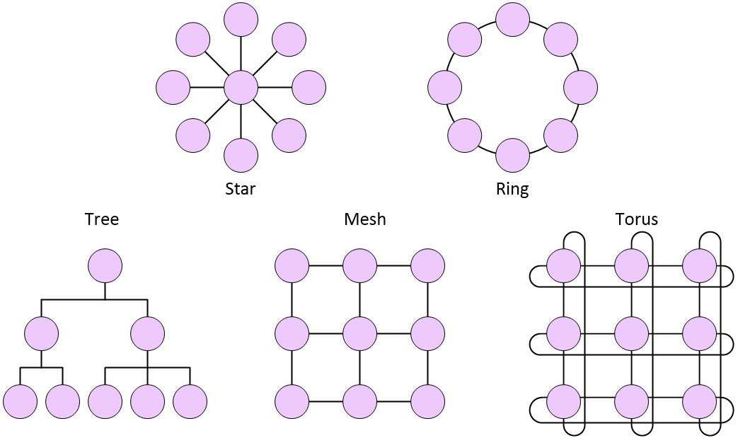
Example NoC topologies (Source: Max Maxfield)
Now, as you may recall, the title of this column is “Artificial Intelligence (AI) Meets Networks-on-Chip (NoCs) in More Ways Than One.” What do I mean by this? I’m glad you asked.
NoCs may be thought of as chip-spanning IPs. Recently, I was chatting with the folks at Arteris IP. One of their many claims to fame is their family of world-leading coherent and non-coherent NoC interconnect IPs.
So, the first aspect of the AI-NoC combo I wanted to discuss is how Arteris can speed the generation of NoCs in the context of AI accelerators like neural processing units (NPUs). Consider a high-level view of a simple SoC containing an NPU as illustrated below. This NPU will typically be formed from an array of processing elements (PEs).

High-level block diagram of an SoC containing an NPU (Source: Max Maxfield)
In turn, all of these PEs will typically be connected using a NoC with a mesh topology (other NoC topologies will be used in different parts of the SoC).
The array of PEs is implemented using a process known as “soft tiling.” The idea here is that the design team will handcraft the first (“golden”) PE. This may contain its own internal NoC, but that’s not something we need to worry about here. The PE will have an associated network interface unit (NIU), as illustrated in (a) below. This NIU will be used to connect the PE to the external NoC.
 Implementing soft tiling by hand (Source: Max Maxfield)
Until recently, the actual tiling process was largely performed by hand. First, the designers would have to replicate the golden PE by cutting and pasting it to form the array, as illustrated in (b) above. Next, the designers would use the NoC tools to auto-generate the NoC, as illustrated in (c) above. For the NoC to transfer data from source (initiator) nodes to destination (target) nodes, the NIU in each PE must have a unique identifier (ID). Thus, the designers would have to hand-configure the NIUs to have unique IDs, as illustrated in (d) above.
Not surprisingly, this version of the soft tiling process is boring, time-consuming, frustrating, and prone to error. Why frustrating? Well, suppose it’s Friday afternoon, you’ve just finished performing an exhausting episode of soft-tiling, and it’s almost time to go home when your team leader pops up, saying, “I just heard that we have to make a tiny change to the golden PE” (I can only imagine your surprise and delight).
This is why the chaps and chapesses at Arteris recently added an automatic soft tiling capability to their NoC technology. This commences with the design team creating the golden PE as before. Now, however, the NoC tools can auto-replicate the PEs, auto-generate the NoC, and auto-configure the NIUs associated with the PEs. All the designer needs to do is specify the desired dimensions of the array, after which the actual soft tiling takes only a matter of seconds.

NoC-enabled soft tiling (Source: Max Maxfield)
This automatic soft tiling capability makes it easy to accommodate changes to the golden PE (and there are always changes). It also makes it easy to experiment with different array sizes. Pretty tasty, eh? But wait, there’s more! In addition to facilitating the creation of SoCs that can perform AI, the folks at Arteris are also paving the way with their recently introduced AI-powered FlexGen Smart NoC IP.
FlexGen can utilize its machine learning (ML) heuristics to evaluate the SoC design and determine the optimal NoC topologies for various areas of the device. FlexGen also minimizes wire lengths and reduces latencies while adhering to user-defined constraints and specified performance goals. In a crunchy nutshell, this fiendishly clever tool facilitates the following:
- Productivity Boost: FlexGen’s smart NoC generation is 10x faster than traditional NoC flows, shortening SoC (or chiplet) iterations from weeks to days for design efficiency.
- Expert-Level Results: FlexGen’s smart NoC technology provides 3x improvement in engineering efficiency with minimal effort and expert-quality results. FlexGen’s algorithms minimize routing congestion, improving silicon area during physical design, with proven links to physical synthesis and place-and-route, thereby supporting tapeout success.
- Wire Reduction-Driven Performance: FlexGen’s smart AI heuristics utilize ML technology to deliver optimized NoC topologies with an average wire length reduction of over 20%. This reduces overall latency by over 10% and provides power improvements across the entire SoC.
The mindboggling growth in SoC complexity has pushed traditional NoC design methodologies beyond their limits. The sophistication of these devices is surpassing our ability to create NoCs without smart assistance. Capabilities and tools like soft tiling and AI-powered smart NoC IPs help to automate and optimize the NoC generation process.
All I can say is that I’m jolly excited by all this. But it’s not all about me (it should be, but it’s not), so what do you think? As always, I’d love to hear any thoughts you’d care to share in the comments below.


