

The awesome new AMD devices to which I’ve just been introduced have sparked a trip down memory lane (I know you’re surprised, because I pride myself on my laser-like focus that prevents me from wandering off into the weeds). I remember the 1970s and early 1980s when we thought the simple programmable logic devices (PLDs) of the time were so cool. Those were heady days when chip manufacturers tried to outdo each other by constantly coming up with new architectures based on different incarnations of AND and OR arrays. The chips’ creators also had lots of fun conceiving new acronyms based on the same handful of letters, such as programmable read-only memory (PROM), programmable logic array (PLA), programmable array logic (PAL), generic array logic (GAL), etc.
There was a variety of underlying implementation technologies, including antifuse and EEPROM, but the one that was dearest to my heart was that of fusible link. In this case, the device was “programmed” by applying pulses of relatively high voltage and current to its inputs to selectively remove (“blow”) tiny internal fuses/links.
Most integrated circuits (ICs) at that time—I’m thinking 7400-series bipolar junction transistor (BJT)-based and 4000-series CMOS-based—were “frozen in silicon.” The fact that you could configure PLDs to perform almost any collection of logical functions you required was awesome. We used these little scamps for all sorts of things, like simple look-up tables and simple finite state machines (FSMs), to gather bunches of simple “glue logic” functions together, and to provide a way of re-working the board in the future if we’d messed something up (it was faster, cheaper and easier to swap out a socketed PLD than to cut tracks and add jumper wires or—horror of horrors—re-spin the board).
Of course, those days were the “Dark Ages” as far as electronic design automation (EDA) was concerned. In the case of PLDs, for example, a typical process commenced by sketching out the desired functionality as a gate-level schematic or state machine diagram using pencil and paper.
This diagram was used as the basis to create a tabular equivalent that was entered as a text file into the device programmer. In turn, this required the designer to have an intimate knowledge of the selected device’s architecture and internal fuses. It also required an in-depth knowledge of the file format required by the programmer. Just for giggles and grins, each PLD vendor defined their own file format that worked only with their own programmer and devices. Oh, the fun we had.
In the early 1980s, a variety of standard PLD languages, file formats, and programming tools arrived on the scene. Names like JEDEC, PAL Assembler (PALASM), Advanced Boolean Expression Language (ABEL), Common Universal tool for Programmable Logic (CUPL), and Automated Map and Zap of Equations (AMAZE) will trigger a wry grin for many older readers.
One of the great things about PLDs was that their timing was deterministic. Their data sheets went so far as to provide input-to-output delays for both rising and falling edges on the inputs causing rising or falling edges on the outputs (now, that’s deterministic).
I remember when Xilinx announced the concept of the field-programmable gate array (FPGA) in 1984, introducing the first device to the market in 1985. The device in question was the XC2064, which contained an 8 x 8 = 64 array of configurable logic block (CLB) “islands,” each with two 3-input lookup tables (LUTs), in a “sea” of programmable interconnect. Unfortunately, this predated appropriate synthesis and mapping (place-and-route) type technologies, so users had to do everything by hand. In turn, this meant that you couldn’t determine input-to-output delays with any level of accuracy until you had a programmed device sitting on your workbench (now, of course, you tell your tools what delays you want and they “make it so”).
“These devices will never catch on,” I remember thinking to myself, which gives you a clue that you should not invest your life savings based on any of my predictions and pontifications.
Altera and Xilinx were founded around the same time, in 1983 and 1984, respectively. Since that time, they both grew to be the behemoths of the FPGA industry. Altera was acquired by Intel in 2015. Intel fought long and hard before they persuaded me to stop saying Altera and instead say Intel Programmable Solutions Group (PSG). Earlier this year, just as I finally had the “PSG” moniker rolling off my tongue, showing that those who don the undergarments of authority and stride the corridors of power at Intel have an impish sense of fun, they announced that the PSG group was to be spun off as a wholly owned subsidiary called… Altera (and people wonder why I drink).
Meanwhile, AMD acquired Xilinx in 2022. At first, they called the group “AMD Xilinx”; today, they prefer that we just say “AMD”; and, as for tomorrow… I’m scared to think.
The reason I’ve taken this long and winding road to get here (yes, of course we’re all thinking of (a) the Beatles and (b) the 2019 movie Yesterday) is that I firmly believe having both Altera and Xilinx is the best thing that could have happened to the FPGA industry. This is because they’ve spurred each other on to create bigger and better devices with increased functionality, capacity, and performance). Speaking of which… (cue “segue-to-die-for” music)…
…I was just chatting with Manuel Uhm (Holistic High-Tech Marketing Executive) and Stephane Gauthier (Product Manager) at AMD. I fear I can hear you exclaiming, “Yes! Finally! He’s getting to the point!” I’d advise you not to take anything for granted because the day is yet young.
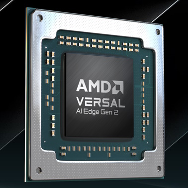
Manuel and Stephane did their best to bring me up to date with their latest and greatest offerings, which were formally announced just a couple of hours ago as I pen these words. In a crunchy nutshell, the guys and gals at AMD are introducing two new series of devices—Versal AI Edge Series Gen 2 for artificial intelligence (AI)-driven embedded systems and Versal Prime Series Gen 2 for classic embedded systems.
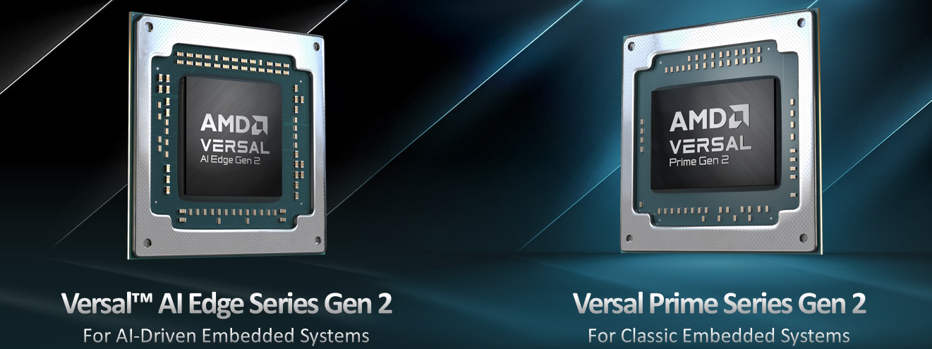 Single-chip intelligence for embedded systems (Source: AMD)
I’m a bear of little brain, so I tend to think of the Prime Series as being like the AI Edge Series without the AI part. And, since AI is appearing in just about everything these days, I’m going to focus on the AI Edge Series here.
There are three phases of processing in AI-driven embedded systems: preprocessing, inference, and postprocessing. Preprocessing encompasses everything that needs to take place to prepare real-world inputs for inference. This can include sensor interfacing, basic data acquisition, standard processing functions (such as image processing), sensor fusion, custom preprocessing, conditioning data for the desired inference model, and more.
AI Inference is what you’d expect; it involves taking the preprocessed real-world inputs and applying standard or custom AI models for perception, analytics, etc. Postprocessing refers to everything that needs to happen to make decisions and take action based on the inference results; for example, behavior planning, vehicle control, and driver display in an autonomous vehicle. All three of these phases require acceleration in today’s high-performance embedded systems.
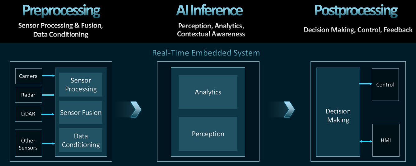 The three phases of processing in AI-driven embedded systems (Source: AMD)
Preprocessing is best handled by programmable logic. AI inference is best performed by a dedicated vector processing engine (or engines). And postprocessing requires high-performance scalar processing engines in the form of embedded CPUs.
Some chip vendors have offerings that focus on only one of these domains. Some gather two of the domains together (preprocessing + inference or inference + postprocessing) while humming the tune to Meat Loaf’s Two Out of Three Ain’t Bad to themselves. However, the optimal solution is to gather all three domains into a single device, as embodied by the Versal AI Edge Series Gen 2 parts, which offer world-class adaptive compute with AMD programmable logic, up to 3X* TOPS per watt with next-generation AI engines, and up to 10X* scalar compute with new high-performance CPUs (*compared to existing Versal devices).
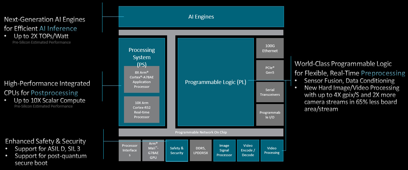 Second-generation Versal Adaptive SoCs deliver end-to-end acceleration in a single device (Source: AMD)
What we are talking about here is up to 8X Arm Cortex-A78AE Application Processors (APs), up to 10X Arm Cortex R52 Real-Time Processors (RUs), and up to 144 AI Engine-ML V2 tiles with up to 72 Mb of data memory and up to 288 Mb of shared memory. Also, the control logic for the AI Engines has been hardened and moved into the AI block itself (previously, this had to be implemented using the programmable fabric). In the case of the Programmable Logic (PL), we have up to 1,188,040 System Logic Cells (SLCs) with up to 543,104 Look-Up Tables (LUTs), up to 2,064 Digital Signal Processing (DSP) engines, up to 16.6 Mb of Distributed RAM, up to 47.2 Mb of Block RAM, up to 33.2 Mb of UltraRAM, and… words fail me.
Manuel and Stephane tell me that all of this is built on a foundation of enhanced functional safety and security, including support for NIST-standardized Post-Quantum Cryptography (PQC) secure boot.
It’s important to note that these second-generation Versal AI Edge Series Gen 2 devices are not intended to replace the first generation, but instead to extend the entire portfolio’s computational, application, and market footprints.
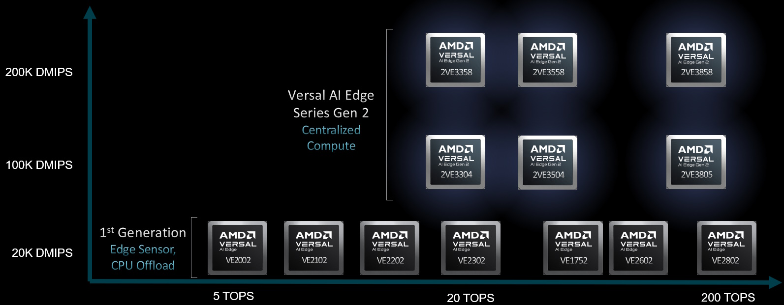 The new second generation devices expand the Versal portfolio (Source: AMD)
Where these new devices really score over their predecessors is in Dhrystone MIPS (DMIPS). This is, in part, achieved by offering new native data type support, including FP8, FP16, MX6 and MX9, where the “MX” types feature shared exponents, thereby reducing the number of bits per element.
It’s also important to note that these new devices are geared up to handle applications that demand Safety Integrity Level (SIL) 3 and Automotive SIL (ASIL-D) risk classification and certification.
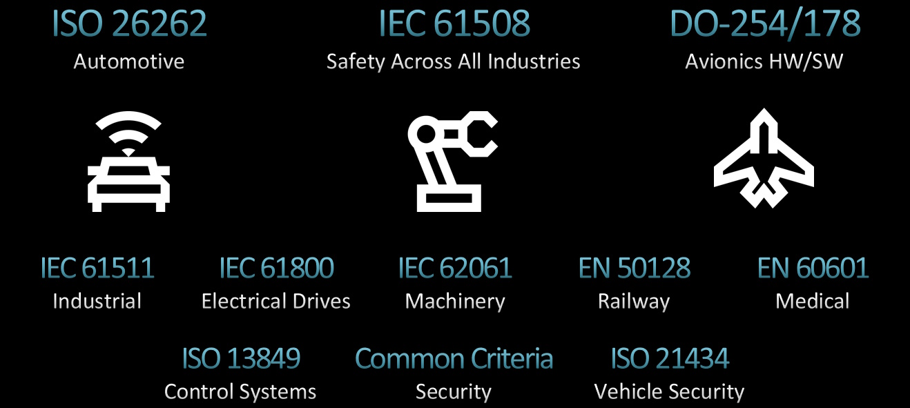 Versal AI Edge Series Gen 2 devices have us covered (Source: AMD)
In fact, this impinges on the programmable network-on-chip (NoC), which is used to connect everything together. The reason for the “programmable” qualifier (which is achieved by means of a NoC Compiler utility) is to prevent stalling and to provide guaranteed bandwidth and quality-of-service (QoS). Also, the folks at AMD have added redundancy in the NoC path from the Processor System (PS) to the DDR memory controllers to achieve ASIL-D and SIL 3 random fault safety levels.
Last, but certainly not least, we shouldn’t neglect AMD’s design tools for these devices. These tools support designers working at multiple levels of abstraction, from Vivado for hardware developers working with Verilog and/or VHDL RTL, to Vitis for software developers working with C++, to Vitis AI for AI and data scientists working with PyTorch, TensorFlow, ONNX, Triton, etc.
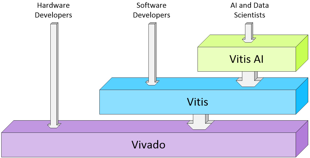 Multi-layered tool stack (Source: Max Maxfield)
I tell you; if I had any idea that this was where things would end up back in 1984 when the folks at Xilinx started talking about their first FPGA… I would have bought a lot of Xilinx stock! How about you? What do you think about all of this?


As crazy noel ideas for programmable logic go, no one can can get close to coming to within a light-year of holding a candle to “3-Body Problem” guys: entangle a pair of protons, unroll them from 11-dimensional space into gigantic 2-dimoensional shell – design a code and write it bit-by-bit into each planck lenght fragment of the shell, (AND THEN DEBUG IT!), then roll them back and send one of the pair to earth and use its entangled twin for instant remote viewing.
WOW! 🙄🙄🙄
* [3-body problem]( https://www.youtube.com/playlist?list=PLDWJ213d2Ucr-3q9LDF9P1_j3Rr3GMJeS )
* [The INSANE History of Netflix’s “3 Body Problem”]( https://odysee.com/@UpperEchelonGamers:3/the-insane-history-of-netflix's-3-body:f )