


If you use low-cost – er – cost-effective FPGAs, there’s great news. You’ll have more choices sometime next year. AMD has just provided more details on its Spartan UltraScale+ FPGA family, based on TSMC’s 16nm FinFET process. These FPGAs will directly compete with Altera’s Agilex 3 FPGAs, when they appear. When it declared its independence from Intel on February 29, Altera reiterated a commitment to extend the Agilex FPGA architecture down from the mid-range Agilex 5 parts to a new FPGA subfamily called Agilex 3. Last September, when Intel PSG fist pre-announced its Agilex 3 plans, I wrote:
“The Agilex 3 family includes B- and C-Series devices. Agilex 3 B-Series FPGAs have higher I/O density and are housed in packages with smaller footprints. They also consume less power than Intel MAX® 10 FPGAs. Agilex 3 B-Series FPGAs target board- and system-level management functions, including Intel’s server platform management (PFM) applications.”
So far, that’s all we know about Agilex 3 FPGAs.
AMD pre-announced the Spartan UltraScale+ FPGA subfamily in a very short blog last June but provided no details. On March 5, the company provided far more details in yet another pre-announcement. Considering that AMD has yet to get first silicon for these parts from TSMC, it will be a while before you see the packaged FPGAs. Documentation is available now, the devices will be added to AMD’s Vivado tool suite in the fourth quarter of 2024, and samples will be available in the first half of 2025.
Nevertheless, AMD has been very generous with additional information in this pre-announcement. There will be eleven members in the Spartan UltraScale+ subfamily, as summarized in the following table:
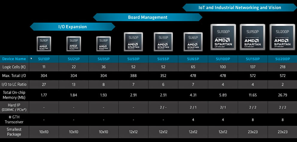
AMD’s new Spartan UltraScale+ FPGA subfamily includes 11 planned members with 11K to 218K logic cells and 304 to 572 I/O pins. Image credit: AMD
Like previous generations of the low-end Spartan FPGA families, the new Spartan UltraScale+ FPGA subfamily is I/O heavy, which means that devices in the family have more I/O pins and fewer logic cells. These devices are designed for I/O-centric applications such as microprocessor I/O expansion, or, as it’s more exotically described these days, sensor fusion.
As you can see from the above table, the smallest Spartan UltraScale+ FPGA has only 11K logic cells but sports 304 I/O pins. This sort of I/O density can be achieved only with specialized packaging. Spartan UltraScale+ FPGAs will be offered in chip-scale packaging with 0.5mm ball pitch and in larger, more conventional BGA packages. The 10x10mm chip-scale packages are intended for designs with severe real-estate limitations. Larger members of the Spartan UltraScale+ FPGA subfamily have as many as 20x the number of logic cells and as many as 572 I/O pins compared to the smallest member of the device family. Incidentally, these are 3.3V-capable I/O pins.
Additional features of note for the Spartan UltraScale+ FPGAs include support for the MIPI D-PHY camera interface at 3.2Gbps, four or eight 16.3Gbps SerDes transceivers in larger members of the FPGA subfamily, and as much as 26Mbits of SRAM in the form of block RAMs (BRAMs) and UltraRAM. All Spartan UltraScale+ devices incorporate DSP48E2 blocks in their FPGA fabric, with 384 DSP blocks in the largest Spartan UltraScale+ device. These DSP blocks are capable of performing fixed-point and floating-point math.
The focus on I/O density enables significant cost reductions when compared with AMD’s Spartan 7 and Artix 7 FPGAs, as shown in the figure below. For a hypothetical design that needs 210 GPIO pins (I don’t know why AMD picked that number of I/O pins), you need to use a Spartan 7 7S50 FPGA with 52,160 logic cells. If your design doesn’t need nearly that many logic cells, you can get more than enough GPIO pins for this design using the smallest Spartan UltraScale+ FPGA, the SU10P, which has just 11K logic cells. You’ll save board space and reduce BOM cost with this change to a Spartan UltraScale+ device.
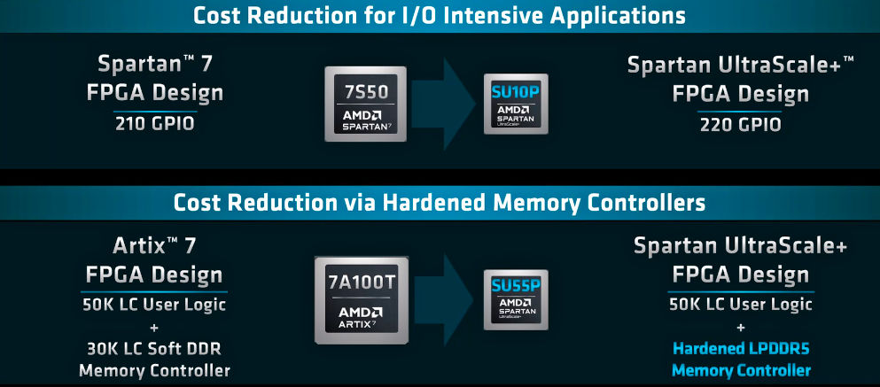
Features added to the Spartan UltraScale+ FPGAs can achieve cost reductions because of their high I/O-to-logic-cell ratios and their hardened on-chip controllers. Image credit: AMD
The lower half of this figure illustrates another way to reduce the cost of a design by using the hardened IP blocks in the Spartan UltraScale+ FPGAs. As shown in the product table above, the largest Spartan UltraScale+ FPGAs incorporate hardened LPDDR5 SDRAM and PCIe Gen4 x8 controllers. For a hypothetical design that requires a DDR SDRAM controller, you’d need 30K logic cells in an Artix 7 FPGA to create a soft SDRAM controller, in addition to 50K logic cells for the hypothetical design in this example. That’s a total of 80K logic cells, which would require an Artix 7 7A100T FPGA. The five largest Spartan UltraScale+ FPGAs each contain two hardened LPDDR5 SDRAM controllers, which cuts the hypothetical design’s logic cell budget by a whopping 30K logic cells and permits the same design to be placed in a Spartan UltraScale+ SU55P FPGA.
Security is often overlooked, especially in designs using low-cost FPGAs. Spartan UltraScale+ FPGAs are only the second family of AMD programmable logic devices to have NIST-approved, post-quantum security built into the FPGAs’ bitstream circuitry. In addition to the low-end Spartan UltraScale+ FPGAs, only AMD’s high-end Versal ACAPs have post-quantum bitstream security. (ACAP is AMD’s fancy name for FPGAs with AI engines and other hardened accelerators.) The Spartan UltraScale+ FPGAs also have on-chip, tamper-resistant circuits that will literally degrade the device if a tampering attempt is detected.
Because Altera has disclosed no details about its Agilex 3 FPGA subfamily, AMD’s announcement now gives Altera the opportunity to tweak its specifications for its new low-end FPGAs. I can’t say for certain that Altera would do this, but it would be silly for Altera to ignore this new information that AMD has provided.
In addition to existing low-end FPGAs in AMD’s Spartan 7, Artix 7, and Artix UltraScale+ device families, other low-end FPGA choices include Altera’s low-end Cyclone FPGA families, which are admittedly getting long in the tooth, and the Lattice Certus-NX, CertusPro-NX, and MACHXO5-NX device families. Microchip also offers several FPGA families in the low-end arena as do Gowin and Efinix. Designers of systems requiring low-end FPGAs have never had so many choices.
References
Steven Leibson, “Intel Heats Up and Expands its Agilex FPGA family,” EEJournal.com, October 13, 2023


I was getting up to my working temperature range to mock them, but it seems that, judging by the Artix UltraScale+ line, prices for lowest-end Spartan subline of UltraScale+ might in fact be priced reasonably this time.
What a surprise from Xilinx. No need for selling one’s blood, kindey and liver to get to these things. Imagine that.
On top of that, it seems that one will FINALLY able to get an FPGA for mere mortals that actually has PCIev4 SERDES and is this capable of decent link to a PC without wasting whole PCIev5 x16 port on a machine for PCIev2x4 link, thus wasting 96+% of the bandwidth. And usually the only good PCIe slot on the machine.
On top of that, Xilinx is sole name that has at least in principle partial SELF reconfiguration capability – that programmed logic in FPGA can reconfigure itself.
On the first glance, it looks VERY nice.
Only other name that has been promising PCIev4 was Efinix (TItanium line) but so far its unobtanium.
Other name was Microchip. PolarFire II was supposed to do fundamental redesign and upgrade all over the place and offer also SoC version with upgraded cluster of RISC-V cores 🥰, but MC got all of the sudden cold feet about it and all talk about it has gone crickets…
So the only other option remains altera with their Agilex 3 line, but somehow I doubt they will be able to top that. OTOH, they might offer aggressive pricing…🙄