


I sometimes joke that I’d bend over backwards to be flexible and that I’d give my right arm to be ambidextrous (I didn’t say they were good jokes). Now, following a recent excursion into wibbly-wobbly analog space (where no one can hear you scream), I’m tempted to say that I’d jump through hoops to be more agile.
I know, it’s a bit weak, isn’t it? Mayhap you could suggest something a tad more rib-tickling (or not, as the case might be), but we digress…
The reason for my desperate attempt to make a play on the word “agile” is that I was just chatting with Chris Morrison, who is the Director of Product Marketing at Agile Analog. Don’t let the “marketing” part of his job title fool you, because Chris has an engineering degree in computer and electronic systems from the University of Strathclyde and a master’s degree in system level integration from the University of Edinburgh (and Scottish degrees are almost as good as their English counterparts LOL).
As I’ve mentioned on occasion, I’m a digital logic design engineer by trade (it’s easy to recognize us by our rugged good looks, chiseled jaws, and confident strides). So, how did it come to pass that I would be found conversing with someone who hails from the dark side (you can identify practitioners of the analog arts by their stooped shoulders, furtive looks, and nervous dispositions)? Well, as much as it pains me to say this, when we are building a state-of-the-art system-on-chip (SoC) device, the vast majority of which is digital, there are still going to be some analog elements in there.
The sort of things we are talking about here are foundational analog functions that every chip needs, such as voltage references and voltage threshold comparators. Also, general sensors such as IR drop (voltage drop) and temperature, along with security-related sensors to detect voltage glitch and temperature glitch attacks. But wait, there’s more, because we will also need things like low-dropout (LDO) regulators and—of course—analog-to-digital converters (ADCs) and digital-to-analog converters (DACs).
Let’s assume we’ve already settled on a foundry, process, and node for our new SoC. On the digital side of the divide, we will go to third parties to purchase digital intellectual property (IP) for standard functions like processors and peripherals, thereby leaving us free to focus on our own internally developed “secret squirrel” IP that will differentiate our SoC from competitive offerings. But from whence can we procure any analog functions we require?
Some SoC teams are replete with digital logic designers but have no analog circuit design capability whatsoever. Other teams do have analog expertise, but they will typically use this expertise to develop the “secret analog sauce” that will distinguish their SoC offering from those of their competitors. In the case of foundational analog IP functions, it’s common for the team to take advantage of third-party analog IP providers, but therein lies the problem…
Due to the fundamental characteristics of analog systems, what we might refer to as “standard analog IP” is far less useful to chip designers than are its digital IP counterparts. In the case of a sensor, for example, the requirements in relation to parameters such as sensitivity, accuracy, precision, linearity, and stability over temperature differ from application to application. Meanwhile, the behavior of an analog circuit will vary substantially from one process and node to another. As a result, an IP that’s perfect for one application when fabricated at one foundry on one process and node may be less than optimal for a different application fabricated at another foundry on another process and node.
As Chris explained things to me, one way to visualize this is to envision the requirements for a piece of foundational analog IP as being like a round hole. Most analog IP companies have an off-the-shelf collection of IP functions, and they will make some effort to customize these functions to meet their customer’s requirements, but the results are still akin to trying to hammer their square pegs into our round holes, thereby leaving us “stressed depressed lemon zest,” as they say.
By comparison, the guys and gals at Agile Analog have created a cunning tool and associated methodology called Composa. “How cunning?” you cry. In fact, this tool is so cunning we could pin a tail on it and call it a weasel (as Black Adder might say) because it makes our lives “easy peasy lemon squeezy,” and it’s not often we are lucky enough to find ourselves saying this these days.
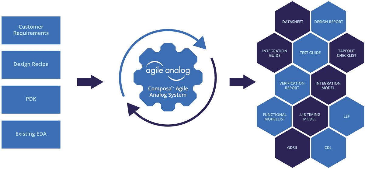
Meet the Composa analog IP creation tool and methodology (Source: Agile Analog).
The way this works is that the customer starts by selecting one of the foundational analog functions found in Agile Analog’s IP portfolio. The customer also specifies their requirements associated with this IP (area, power consumption, speed, sample rate, sensitivity, accuracy, precision, linearity, stability over temperature, etc.). Furthermore, the customer specifies the foundry (all major foundries are supported, including TSMC, GlobalFoundries, Samsung, and SMIC), process (CMOS, FDSOI, FinFET), and technology node (from 180nm and above to 5nm and below).
Composa accepts as inputs a seed design (a.k.a. “design recipe”) for this function (these seed designs are handcrafted by the analog artisans at Agile Analog), the customer requirements, and the foundry’s process design kit (PDK), and it uses sophisticated self-acting and systematic algorithms to determine the optimal implementation. Automatically generated, correct-by-construction deliverables include a data sheet, design report, integration guide, test guide, tape-out checklist, verification report, integration model, functional model, timing model, and all the files needed for tape-out (GDSII, CDL, and LEF).
Save Room for the Main Course
Another one of my little jokes (and this one really is quite funny) is when my wife (Gina the Gorgeous) and I invite friends around to our house for a dinner party. We start by serving a sumptuous selection of little nibbles as appetizers. These are followed by a reasonably-sized entrée (not overly large because of all the nibbles). As our guests are starting to slow down as they near the end of the entrée and see the finishing post (in the form of the dessert tray) in sight, I usually say, “make sure to save room for the main course.” You should see their faces.
The reason I mention this here is that everything we’ve discussed thus far is equivalent to the appetizers leading up to the main course, which is taking groups of the aforementioned foundational analog IP functions and gathering them together into analog subsystems.
Chris told me that, as part of the current spate of RISC-V adoption and ensuing RISC-V-based designs, the folks at Agile Analog have been seeing a bunch of newer, smaller companies dipping their tippy toes into the SoC design waters. Chris notes that many of these companies are comfortable with the digital portions of the design but struggle with the analog side of things.
Apart from anything else, grouping analog functions in this way offers advantages in terms of size and power. It’s a bit like assembling a jigsaw puzzle. The expert analog designers at Agile Analog can fit the functions together in such a way as to minimize silicon real estate. Also, knowing that an IP being driven is abutting the IP doing the driving allows the designer to minimize the drive strength (current and power) of the driver.
But wait, there’s more… for example, any signals from sensors in the analog realm must be converted into their digital equivalents for use in the digital domain. This moves us into the area of mixed-signal design and verification, which can bring the strongest amongst our number to their knees. Suffice it to say that it’s not as simple as slapping an ADC between the sensor and the rest of the SoC—there are all sorts of sampling rates and metastability issues to wrap one’s brain around.
This explains why, in order to add a great big dollop of metaphorical cream on top of our zero-calorie allegorical cake, the heroes and heroines at Agile Analog have encapsulated their analog subsystems with digital wrappers (am I the only one who is currently thinking about the BRILLIANT! adverts for Guinness?).
The folks at Agile Analog are interface agnostic, so these digital wrappers support a variety of interface protocols, including Arm’s AMBA APB and SiFive’s TileLink. As Chris says, “As long as it’s something we can get the specification for, we can create the RTL to support it.”
In addition to allowing the main SoC to read data from analog sensors, the digital wrapper also allows the SoC to write data into the subsystem’s configuration and control logic, like defining sequences in state machines, setting threshold levels on programmable comparators, and specifying voltage levels on LDO regulators, for example.
Three of these subsystems have been announced so far, with more to follow. These new subsystems are the agilePMU Power Management Subsystem, the agileSMU Sleep Management Subsystem, and the agilePVT Sensor Subsystem, where PVT stands for process, voltage, and temperature. Each of these subsystems can be customized with respect to the number of channels they support (e.g., the number of LDOs in an agilePMU and the number of voltage comparators in an agileSMU).
In this context, power management includes powering up (and down) different design functions in appropriate sequences. To be honest, until now, I’ve only ever really considered power management in the context of the board level; that is, powering up (and down) chips in the right order. It simply had not struck me that this was something one might also wish to do with respect to the various IP functions in an SoC. In addition to its digital wrapper, the agilePMU Power Management Subsystem is equipped with an integrated digital controller that offers precise control over start-up and shutdown, supports supply sequencing, and allows for individual programmable output voltage for each LDO. Furthermore, status monitors provide real-time feedback on the current state of the subsystem, thereby ensuring optimal system performance.
If the SoC is designed in such a way as to support a low-power sleep mode, then the agileSMU Sleep Management Subsystem is going to be of interest. In addition to one or more programmable oscillators for low frequency SoC operation, including a real-time clock (RTC), this subsystem includes low power comparators that can be used to initiate the wake-up sequence, along with a power-on-reset (PoR) that provides a robust, start-up reset to the SoC. Once again, the agileSMU is equipped with an integrated digital controller that offers precise control over wake-up commands and sequencing. And, once again, status monitors provide real-time feedback on the current state of the subsystem, thereby ensuring optimal system performance.
Last, but certainly not least, we come to the agilePVT Sensor Subsystem. The monitoring of process, voltage, and temperature variations is critical when it comes to optimizing power and performance for modern SoCs, especially those realized using advanced node and FinFET processes. The agilePVT Sensor Subsystem is a low-power integrated macro consisting of process, voltage, and temperature sensors, along with an associated reference generator, for the on-chip monitoring of a device’s physical, environmental, and electrical characteristics.
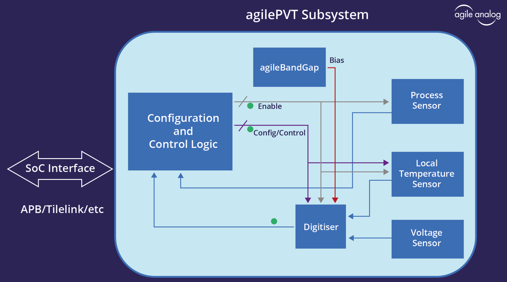
Meet the agilePVT subsystem (Source: Agile Analog)
As for the other subsystems, the agilePVT Sensor Subsystem is equipped with an integrated digital controller that can be used to provide precise control. Meanwhile, status monitors provide real-time feedback on the current state of the subsystem, ensuring optimal system performance over the full product lifecycle.
Since voltage and temperature can vary across the die, SoC designers typically employ several of these subsystems in appropriate locations. When it comes to process, this refers to variations caused by minute dissimilarities in materials and slight disparities in the various manufacturing process steps. When I wore a younger man’s clothes, we considered process variations only in a wafer-to-wafer context. As geometries grew smaller and tolerances grew tighter, it became necessary to consider process variations between dice on the same wafer. These days, we are obliged to consider the fact that process variations can be significant across the face of a single die; furthermore, these variations can evolve over the lifetime of the chip. “Eeek Alors!” is all I can say to that (and I mean this most sincerely).
Now, much like Winnie the Pooh, I may be a bear of very little brain, but it doesn’t take me long when looking at the above diagram to realize how the temperature and voltage sensors fit into the picture. (Having said this, measuring temperature is not as easy as many people might think, as I discussed in What the FAQ are Celsius and Fahrenheit? and What the FAQ are Kelvin, Rankine et al? and How to Measure Things Like a Canadian.)
But what about the “Process Sensor” block? How does one go about measuring process variation “on-the-fly” in the middle of an SoC? This is another topic that had never previously bid a cheery “hello” to the little grey cells in my brain. Chris enlightened me by explaining that this sensor involves a ring oscillator with delay cells. Analyzing the oscillator’s operation allows us to determine what’s going on process-variation-wise with respect to the PMOS and NMOS transistors forming it. I can’t help myself, I’m back to hearing Guinness’s BRILLIANT! adverts bouncing around (what I laughingly refer to as) my mind.
Well, I don’t know about you, but I’m very impressed, and that’s not something you can expect to hear me say often about anything analog. How about you? Do you have anything you would care to share on the topic of analog IP used in SoCs?


