


Well, the hot news on the street this week — if you live on a street where people are scampering around performing hardware acceleration on their algorithms — is that those clever guys and gals at Achronix , who announced their state-of-the-art 7nm Speedster 7t FPGAs a couple of months ago, have teamed up with the creative chaps and chappesses at BittWare (a Molex Company), who just announced their VectorPath S7t-VG6 accelerator card.
I was just chatting with the folks from Achronix and BittWare, who are bouncing off the walls with excitement because they say that this little beauty is a new class of FPGA accelerator. This card — along with its supporting tools and ecosystem — is designed to reduce time to market when developing high-performance compute and acceleration functions for artificial intelligence (AI), machine learning (ML), networking, and data center applications (see also Fundamentals: AI, ANNs, ML, DL, and DNNs).
But why do we need accelerator cards in the first place, why are FPGA-based accelerator cards of particular interest, and what makes this one so special? Well, I was hoping you would ask me these questions, so thank you for giving me the opportunity to expound, explicate, and elucidate (don’t worry; I’m a professional; it’s not as painful as it sounds).
Why do we Need Accelerator Cards?
I am a huge supporter of the honking big microprocessors (MPUs) used to power workstations and servers. If they had a fan club, I’d be the president.
MPUs are fantastic when it comes to solving certain problems and implementing decision-making logic (“If someone opens window A, strobe light B and sound alarm bell C”). Sad to relate, however, MPUs really aren’t that efficient when it comes to performing certain algorithms, such as those requiring the same operation to be performed on multiple pieces of data (they just appear to be fast because we are clocking them at approximately the same frequency as a microwave oven).
Suppose we wanted to perform an addition operation on 10,000 pairs of integers, for example. The way this works is that the central processing unit (CPU) in the MPU fetches an instruction, then it decodes that instruction, then it fetches the associated data, then it performs the desired operation, and — finally — it stores the result. But wait — there’s more, because now the CPU has to repeat this operation another 9,999 times!
By comparison, if implemented in a massively parallel fashion using suitable hardware, the same 10,000 additions could be performed in a single clock cycle (this is a drastically simplified description that omits the fiddly details, including any overheads involved in moving the data around, but it serves the purpose of this example).
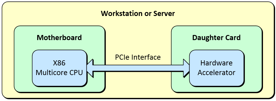
A very common way to implement hardware acceleration is to augment an X86-based motherboard in a workstation or a server with a daughter card connected via a PCIe interface.
A typical flow would be as follows. The original application is created in a software programming language like C/C++, for example. This application is then executed and profiled to determine which functions are consuming the most processing time and acting as bottlenecks. These functions are then translated into a form that can be used by the hardware accelerator. It’s also necessary to implement appropriate interfaces between those portions of the design that are implemented in software and those that are realized in hardware. Even taking this overhead into account, the hardware accelerator can speed performance from 10X to 100X depending on the application.
Why FPGA-Based Accelerator Cards?
Many diverse workloads are driving the need for data accelerators, including extreme computation, networking, storage, and sensor programming.
Some example workloads are as follows (where * characters indicate AI/ML workloads): voice recognition/search*, sentiment analysis*, image recognition*, motion detection*, recommendation engines*, text analytics*, analytics, fraud detection*, financial modelling*, machine translation*, genomics, hashing, high-frequency trading, DPI (deep packet inspection; i.e., opening a packet’s payload to inspect its contents and possibly perform some actions), network monitoring*, server disaggregation, load balancing*, firewalls, NFV (network functions virtualization), SDN (software defined networking), virtual machines, encryption, DDoS (distributed denial of service) detection and mitigation, database acceleration, deduplication, erasure coding, compression, search, weather forecasting, oil exploration, radar, and medical imaging, to name but a few (phew!).
There are several options we could use to implement the hardware accelerator, including graphics processing units (GPUs), FPGAs, and custom-built ASICs/SoCs. (On the off chance this is new to you, a modern GPU can contain thousands of small processors).
For the highest speed and lowest power consumption, a custom integrated circuit in the form of an ASIC/SoC is always going to be the best option… assuming you can afford the tens of millions of dollars and the 12 to 24 months it will take you to design and fabricate the little rascal. Unfortunately, such a solution will be applicable to only a certain class of application problems, because any algorithms implemented in the ASIC/SoC fabric are essentially “frozen in silicon.” This means that you would have to create multiple ASICs/SoCs to address different classes of application problems.
When it comes to GPUs and FPGAs, each may “pip-the-performance-post” for different classes of application problems. At the end of the day, however, when we consider the diversity of workloads presented earlier, the versatility of FPGAs wins the day if your workstations and servers are going to be performing hardware acceleration on a wide range of application problems (see also New Platform Helps Software Developers Realize CPU+FPGA Systems, Using FPGAs to Accelerate C/C++ [Pipelining], and Using FPGAs to Accelerate C/C++ [Loop Unrolling]).
One application that may surprise a lot of people is based on the fact that banks are obliged to perform all of their calculations in decimal. The reason for this is that, while it’s easy to represent certain values like 1/10 = 0.1 exactly in decimal, it’s possible to obtain only a close approximation of these values in binary (the number system used by MPUs), because 0.1 in binary is 0.00011001100110011… (requiring an infinite number of 0011s). The problem here is that the cumulation of lots of small errors due to rounding can creep in, and governments don’t like that, so they’ve mandated that any calculations performed by banks must return the same results as if they were performed using pencil and paper, and the only way to guarantee this is to work in decimal.
Performing arithmetic operations in decimal involves a substantial overhead when using traditional MPUs, and it’s not something GPUs are good at either. The problems are only exacerbated when working with the humongous data sets that are the hallmark of financial institutions. This is one of those tasks where the ability to configure the FPGA’s fabric to implement custom functionality wins the day.
Why the VectorPath S7t-VG6 Accelerator Card?
Let’s start with the Achronix 7nm Speedster 7t FPGA, which resides at the heart of the VectorPath card. The Speedster7t FPGA is optimized for high-bandwidth workloads, and it eliminates the performance bottlenecks associated with traditional FPGAs. Built on TSMC’s 7nm FinFET process, Speedster7t FPGAs feature a 2D network-on-chip (NoC), an array of new machine-learning processors (MLPs) that are optimized for high-bandwidth and AI/ML workloads, high-bandwidth GDDR6 interfaces, and 400G Ethernet and PCI Express Gen5 ports, all of which are interconnected to deliver ASIC-level performance while retaining the full programmability of FPGAs.
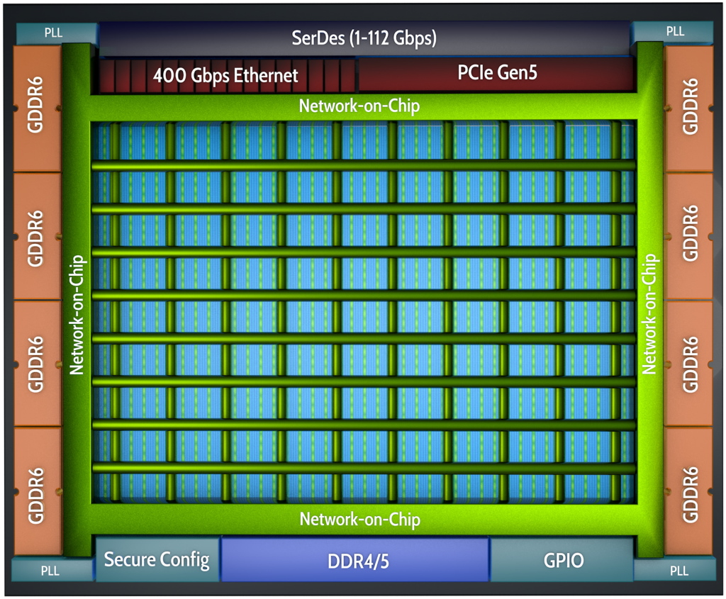
High-level representation of Achronix 7nm Speedster 7t FPGA (Image source: Achronix)
The connections between the network-on-chip (NoC) and FPGA functions are performed by master and slave network access points (NAPs) that are located at every row-column NoC intersection. Each row/column supports 256 bits running at 2 GHz, which equates to 512 gigabits per second. Links operate in both directions, and the theoretical maximum device bandwidth is 20 terabits per second. The connection modes include transactions (AXI), packets (for Ethernet), and raw data streams within the FPGA core.
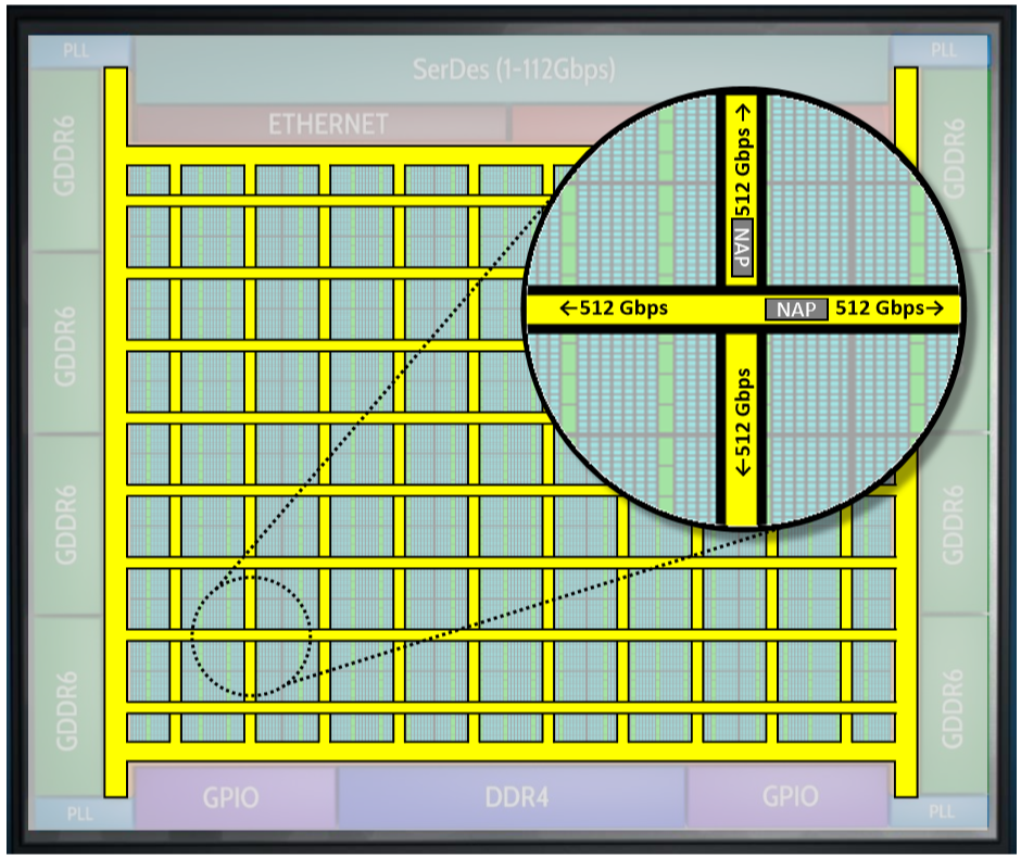
Achronix 7nm Speedster 7t FPGA NoC and NAPs (Image source: Achronix)
Many industries and markets are rapidly adopting artificial intelligence and machine learning (AI/ML) because these probabilistic algorithms are now able to solve a wide range of intractable problems that are not easily addressed by any other approach.
In order to address these algorithms, each Speedster7t FPGA features a massively parallel array of programmable compute elements, which are organized into machine-learning processor (MLP) blocks. Each MLP is a highly configurable, compute-intensive block, with up to 32 multipliers that support integer formats from 4 to 24 bits and various floating-point modes, including direct support for Tensorflow’s bfloat16 format as well as a supercharged block floating-point format, which doubles the multiplier count of the MLP.
The MLP’s programmable MAC incorporates both a fracturable integer MAC and a hard floating-point MAC. Each MLP block in the Speedster7t fabric also incorporates two memories that are hard-wired to the MAC blocks. One memory is a large, dual-ported 72-kilobit embedded SRAM (BRAM72k), and the other is a 2-kilobit (LRAM2k) cyclic buffer. The number of available MLP blocks varies by device, but it can number into the thousands.
Now let’s turn our attention to the VectorPath acceleration card itself. Remember that this was designed as a collaboration between Achronix and BittWare (a Molex company), where the latter has a 30-year track record of successfully designing and deploying FPGA accelerator products. The folks at BittWare modestly claim to be, “The only FPGA-vendor-agnostic supplier of critical mass able to address the qualification, validation, lifecycle, and support requirements of enterprise customers deploying FPGA accelerators in high volumes for mission-critical applications.” (You ought to hear them talking about themselves when they’re not being modest. LOL)
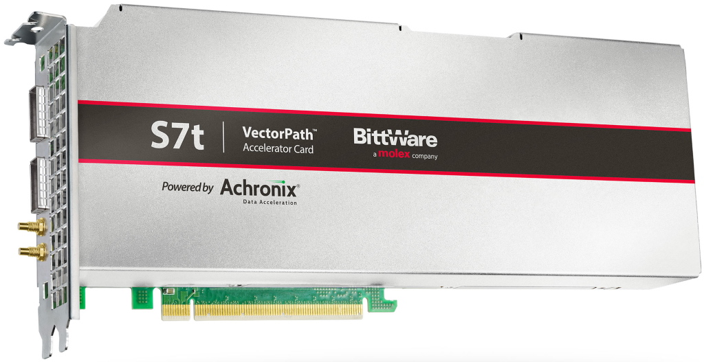
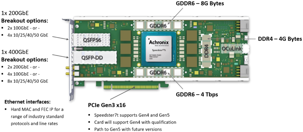
VectorPath S7t-VG6 PCIe accelerator card (Image source: BittWare, a Molex company)
This full-height, double-width, 3/4-length (GPU-size) is going to be made available as a standalone card or as an option to purchase pre-integrated as a DELL or HPE TeraBox server from BittWare. It has to be acknowledged that this bodacious beauty — which will begin shipping at the beginning of Q2 2020 — is a bit of a beast.
The VectorPath’s high-performance interfaces include 1 x 400GbE and 1 x 200GbE interfaces with 8 banks of GDDR6 memory with aggregate bandwidth of 4 terabits per second, thereby making the card ideal for high-bandwidth data acceleration applications. Breakout options for the 1 x 200GbE interface include 2 x 100GbE or 4 x 10/25/40/50 GbE, while breakout options for the 1 x 400GbE include 2 x 200 GbE, 4 x 100 GbE, or 8 x 10/25/40/50 GbE.
VectorPath S7t-VG6 PCIe accelerator card (Image source: BittWare, a Molex company)
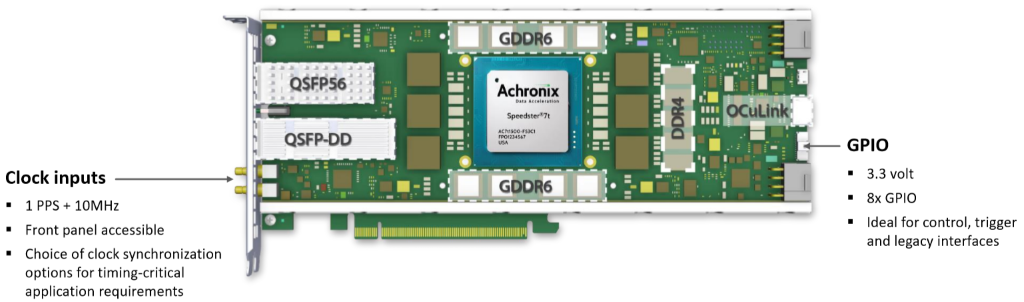
One thing that really impressed me about the VectorPath is that its creators obviously knew what they were doing; for example, they designed it to be scalable from a single card to many-card installations. This is evidenced by things like the clock and GPIO expansion interfaces. In particular, the OCuLink interface supports NVMe access (interface directly with NVMe Flash arrays for database acceleration and big data applications), card-to-card scaling (scale independently of the PCIe bus, with a deterministic, low-latency, high-bandwidth interface), the ability to add extra network ports, and the ability to retrofit older systems by integrating new technology using protocol-agnostic serial I/O.
VectorPath S7t-VG6 PCIe accelerator card (Image source: BittWare, a Molex company)
The VectorPath accelerator card includes a full suite of Achronix’s ACE development tools along with BittWare’s board management controller and developer toolkit, which includes the API, PCIe drivers, diagnostic self-test, and application example designs to enable a rapid out-of-the-box experience.
One final point I’d like to note before I go is that the folks from Achronix and BittWare told me that they recognize that they have to employ a flexible cost model to meet price points at different volumes for different customers. Thus, in addition to off-the-shelf VectorPath accelerator cards, BittWare will offer custom board design services for customers with high-volume requirements. Furthermore, when volumes reach tens of thousands of units, BittWare can allow the end customer to manufacture and test the S7t-VG6 at their preferred CEM under license. Customers can even create their own variants of the S7t-VG6 under license, thereby benefiting from BittWare’s 30 years of expertise and IP.
In Conclusion
I for one am jolly enthused by the Speedster 7t FPGAs from Achronix and the VectorPath S7t-VG6 PCIe accelerator card from BittWare. There are a number of FPGA vendors out there fielding some very tasty devices, but rather than trying to be “all things to all people,” the guys and gals at Achronix have picked a focused set of application areas and target markets with extreme performance requirements and then tailored their FPGA architecture accordingly.
Meanwhile, the chaps and chappesses at BittWare have architected the VectorPath hardware accelerator card to take full advantage of the high-end capabilities of the Speedster 7t FPGA, while also keeping real-world usage models that demand configurability and flexibility into account.
Now I’m sitting here pondering what I would like to accelerate here in my office. How about you? Do you have any data-intensive applications that would benefit from a 10X to 100X speedup?


It amazes me to think about the raw compute power offered by this card — if I got my time machine working and took it back to say 1975… it would be useless because they didn’t have the PCIe interface back then LOL
“Now I’m sitting here pondering what I would like to accelerate here in my office. How about you? Do you have any data-intensive applications that would benefit from a 10X to 100X speedup?”
No, But I think it is time to put some effort into control/decision logic optimization. The memory wall is also a problem.
JIT, RISC, Branch guessing, Speculative execution, Cache coherence, etc. all increase memory accesses.
By utilizing the dual port block memory to execute if/else, do/while, for, and assignments in an FPGA I can eliminate compiling to an ISA or an intermediate language. It takes 4 block memories, and about 500 LUTs to run a basic C program. On top of that the C# Visual Studio is used for debug and the Roslyn Compiler API produces the control logic and variables/values for execution.
It reduces the weasel wording quite a bit. By the way since the inbound data for an accelerator may have entered via an FGPA I wonder why it was written to memory only to be read and sent to the accelerator? Just buffer it or better yet process it (DSP) and save a round trip to memory.
“It takes 4 block memories, and about 500 LUTs to run a basic C program.”
Seriously? Wow! Maybe you should write an article about that (or talk to me and I’ll write it — if you’re interested, email me at max@clivemaxfield.com).