


We all know that security is bubbling its way up in importance, and we all probably know that key management is an important part of keeping good security. Nothing ruins a good secret like someone discovering the keys.
There are lots of keys that get tossed about in any given transaction, but many of them are derived ephemeral keys used only for a single session or a single transaction. Those keys will all be generated using the master-of-all-keys, and that’s the key that lives on for the life of the system. So it has to be retrievable only with permission. It’s better yet if the key itself can’t be retrieved, but is used only for opaque hardware calculations far from prying eyes.
But there’s still vulnerability when loading such a key. How do you get the key stored in the first place? You can’t send it by encrypted message since you don’t yet have a key for unencrypting the message. So you end up with laborious manufacturing schemes involving trusted machines that load the keys and track which keys were loaded. Fussy but necessary.
Unless… you can use some intrinsic characteristic of a device as a key. This is the domain of the physically unclonable function (PUF). We looked at these in general six years ago. Of the different schemes, SRAM has proven the most lasting, and Intrinsic ID appears to be the chief commercial proponent. This scheme relies on the fact that: a) each SRAM array on a chip powers up with random bit states that are, to a reasonable approximation, unique, and b) that the device powers up the same way every time.
That last piece is mostly true, although there may be some noise in the system as this or that bit comes up wonky here and there. So there may be circuits both to do error correction and to improve the entropy as necessary.
Well, at a press event held just before Imec’s recent technology forum (ITF) in Antwerp, Imec discussed a new PUF mechanism that was worked in conjunction with KU Leuven. Instead of using SRAM bits, they take two transistors next to each other and use a highish voltage to blow the oxide in the gate of one of them. The idea is that the voltage at which one transistor blows will be slightly different from that of the other due to natural variation, so they won’t both blow together. It’s effectively random as to which will blow first.
That means that each pair can be read as a bit – say, left blown is 0, right blown is 1 (or vice versa).
This cell has a number of benefits over an SRAM-based cell.
- It’s non-volatile, so there’s pretty much no chance of the very occasional coming up wrong.
- There are two transistors instead of six.
- It can’t be disturbed by alpha particles and such; it should be radiation-stable.
Of course, one of the main benefits of SRAM is that you already have a bunch of it on chip, and you can even repurpose some of the existing SRAM as a PUF – the point of the previously linked Intrinsic ID article.
This new Imec/KU Leuven PUF wouldn’t appear to require anything unusual in the process technology, but it does require dedicated peripheral circuits. So the question is, what’s the cost of this new PUF as compared to SRAM?
From a hardware standpoint, if you use part of the existing SRAM for your PUF, then you’re leveraging all the read and write hardware – the support circuitry – that you already have, so the cost really is just the loss in individual bits – and the cost in security, since calculations are done in software. No other circuitry is required. But each of those bits needs six transistors – a lot. And they’re designed for fast SRAM performance – not a requirement for a PUF.
So can a new PUF array be created that’s net smaller than either a chunk of SRAM bits or a separate dedicated SRAM PUF array (which would need its own read/write circuitry, but could be made from smaller transistors)? If the cost is a bit higher, is the improved security worth it?
I hoped to have a deeper-dive conversation with someone from KU Leuven, although they were cagey about how much they could discuss. While waiting, I started noodling mentally on how an array like this might be built. Before long, I had come up with my own architecture for how to build it. (No, there’s no way I could design the actual circuits – that’s what you guys do.)
When I went back to get a sanity check from KU Leuven, I didn’t get a response after a few tries. This could mean that they’re too busy to get into that much detail; it could mean “no comment”; it could mean that I got closer than they’d like; or it could mean that I’m so far off it’s not worth spending time on. I really don’t know.
But I thought it might be interesting to take you through my thought process; you can decide for yourself whether it makes sense. And some of you may be able to provide some insights on the sizes of circuits, from which we could compare the cost to that of SRAM. That’s my ultimate question, and it’s one I wasn’t able to answer myself.
Rules of the Road
First, for a given pair of transistors (a single cell): the challenge is to blow exactly one of them, without knowing which. That says to me that:
- You need to sweep a voltage, starting lower than the blow range so that you don’t risk blowing both when you start. The ramp must be gentle enough that, when one cell blows, there’s time to react before the other one goes.
- It would be best if it were self-limiting so that, once one of the pair blows, the voltage comes down and avoids blowing the second one. One way of doing that is to put a resistor in the line feeding the gates. Before anything blows, there’s no current, so there’s no drop across the resistor. As soon as one of them blows, however, the current will cause a drop, immediately lowering the voltage so that the other transistor won’t blow. (Some finessing might be required to ensure a consistently high-quality rupture in the oxide… I haven’t included that…)
- You need to sense the currents of the two transistors separately so that you know which one blew. It might be useful to have a circuit that detects whether either both or neither of the cells programmed (over/underprogram), providing an error signal. That would be optional.
Next, for efficiency, it’s nice to be able to write and read more than one cell at a time. But you can’t do an entire row in parallel, or else, once one transistor goes, then the voltage drops and none of the other cells along the row would program. (I’m assuming one resistor per cell would be too expensive.) You could, however, program multiple cells along a column, since each would have its own row line so that, when a cell blows on one row, it wouldn’t affect any other row
For reading, it’s the opposite. You wouldn’t want to read an entire column for the following reason: If you’re reading only one cell, then you merely have to detect the presence of current; the exact value isn’t important, saving time and circuitry on sensitive sense amps. But if you wanted to read an entire column, then you’d have to figure out how much current there was – and, even then, it would tell you only how many cells were programmed, not which ones. You could, however, read an entire row in parallel, since you’d be measuring only one cell per column.
Here are some points I don’t know.
- What’s the blow voltage range? Are charge pumps needed?
- What’s the size of the array? The bigger the array, the more the efficiency of the individual cell helps to overcome any overhead circuitry (like charge pumps, if they’re needed).
- I don’t know the hashing function that turns the array state into a key. You wouldn’t want to be able to read the array as a whole, or else someone could start reverse-engineering the thing. You want hardware to generate the key immediately for use in some protected way. Then again, it occurred to me that the hashing for this or an SRAM-based approach (if done in hardware) could likely be the same except for possible differences in array dimensions. If an SRAM is hashed by software, it’s better than no security, but it’s more vulnerable (if cheaper) than a hardware solution. So this probably isn’t a comparison point between SRAM and this PUF.
Putting all of that together, those outstanding questions notwithstanding, I came up with the following architecture.
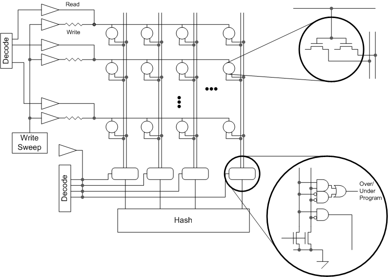
We’ve got some analog blocks on there to sweep (and generate?) the blow voltages. It occurs to me that some sort of weak hold-down would also be needed to ensure that a floating column would reliably read as a 0. (Either that or use a more complex pre-discharge approach…)
It also occurred to me that programming is done once, and it could be done as a final testing step in the factory rather than in the field. That means you could have a test equipment generate the analog voltages (the output of the Write Sweep block), saving lots of space by eliminating circuits that would be used only once. That, however, raises concerns about yet another way to get in and hack (or brick) the chip, so if such an approach were used, you’d probably want a way to permanently disable those lines from the outside so that, once the array was programmed, you could no longer use those signals.
If you did that, then the overhead circuits are more or less the same as what an SRAM has, with the exception of the resistors. So the smaller array seems more likely to win. If the tester interface had enough lines to include one per row, then you might be able to let the tester handle that aspect as well, further shrinking the overhead and giving the nod to this new PUF.
So the remaining big questions are:
- Does a smaller array cell make up for the added analog circuits as compared to a standalone SRAM PUF block (not a repurposed segment of the main SRAM memory)? Or does this win based on a tester generating those voltages?
- Is the entropy better so that you can get away with a smaller array?
- Ultimately, is this cheaper to produce than an SRAM-based block?
Feel free to share any thoughts in the comments.


What do you think of this new Imec/KULeuven PUF?
It’s been several decades since I took the intro VLSI design class, and probably still have my copy of Introduction to VLSI Design. I’m not a chip designer. But there are likely to be several gotcha’s with this process.
The first is assuming these PUF arrays will produce random results when blown. It’s possible the “natural variation” will actually be significantly predictable from wafer to wafer simply because of small mask and/or E-Beam variations. There may be a predictable variation from die to die on a single wafer, along with the chance that the same die position from wafer to wafer will have similar results.
The second is that it would probably take some serious purposeful tinkering with the doping process it introduce defined random feature variations. This is very counter to normal production processes that try very hard to minimize any process variance to improve yields … and depending on variances, does risk failure when process engineers succeed at improving the process yield with better quality controls.
The third is that there is some significant risk that at least part of the die array is partially predictable. Enough so, that the brute force search for the key is significantly reduced in effort. Maybe not for every PUF, but for enough PUFs, that this subset of PUF’s will create significant risks for the product as a whole. This may not appear as a crack, until the devices are all deployed in the field.
I can’t comment on these things myself, but the teams claim to have done a lot of work testing out the entropy, and they say it’s so good that no additional circuits are needed. Obviously they’ll need to put data out there at some point to bolster the case, but, taken at face value, they claim that they have shown that it works.
A couple decades ago the crypto folks declared that SSL was rock solid, yet a number of hacks have proven otherwise since. The leaks disclosing BULLRUN successes, and the NSA’s ties to premier security companies for back doors, does leave me very skeptical about hardware solutions that have large claims. There is always a strong marketing clamor for the appearance of security, reality too often significantly departs from the goal of real security.