


For the last two decades or so, the EDA industry has grown at the same rate as the overall semiconductor industry. Mentor Graphics CEO Wally Rhines explained the situation to Magdy Abadir in the January/February 2017 edition of IEEE Design and Test magazine:
“EDA revenue is very stable at 2% of semiconductor revenue, and if the semiconductor industry doesn’t grow, it’s difficult for the IC design-related parts of the EDA industry to grow. …Historically, EDA grew much faster than the semiconductor industry because not everyone had adopted automation, so we were still filling the seats with more and more software per person. Then we reached a point where everyone had 100% of their design flow automated, and it settled out. We’re now, almost 20 years later, growing at roughly the same rate as the semiconductor industry.”
Frank Schirrmeister, VP of solutions and business development at Arteris, provided a different perspective of the same situation in an article titled “Chasing The Next Level Of Productivity,” which appeared on the Semiconductor Engineering Web site. Using Handel Jones’s IBS reports from 2014, 2018, and 2022, Schirrmeister plotted semiconductor design starts from the year 2000 and used IBS projections to take the plot out to 2030. The plotted data shows design starts growing from slightly over 8000 to slightly over 11000 over the course of that three-decade period.
I’ve adapted Schirrmeister’s data in the chart below.
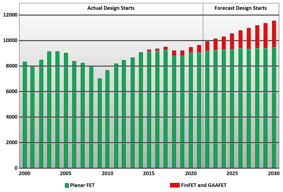
Frank Schirrmeister plotted semiconductor design starts from the year 2000 to 2030 using Handel Jones’s IBS reports from 2014, 2018, and 2022. Image credit: Frank Schirrmeister and IBS
Most of those semiconductor design starts shown in the above chart are for semiconductors designed for older process nodes that are based on planar FETs. Those design starts have been essentially flat since 2015. The real growth in the number of design starts occurs in the nodes with 16nm and smaller geometries – the FinFET and GAAFET (Gate All Around FET) nodes – but the total number of new design starts doesn’t really grow that much. Growth is a dismal CAGR of 1.0672%, which is certainly not enough to sustain the EDA industry’s traditionally high annual growth rate.
In his article, Schirrmeister writes:
“The growth of design starts does not look like an inflection point at first sight in the traditional ‘hockey stick’ sense. Well, not until one multiplies the data out with the effort per technology node and the realization that most of the predicted growth comes from 7nm and beyond. Delving into the data further reveals that the expected development cost almost triples from 7nm to 5nm alone. The cost of prototypes and their validation alone at 3nm and 2nm is as much as the development cost of a whole 16nm design. We do not have enough engineers and cannot educate enough in time to satisfy the design demand, so we are stalling without productivity improvements.”
I submit that “stalling,” this low-growth situation, leaves the EDA industry with no choice but to propel itself into a new era, which I’ve named the Big DA Era. In fact, I assert that there’s an exact date marking the start of this new era: March 30, 2017. On that date, Siemens announced that it had closed the purchase of Mentor Graphics for $4.5 billion. The company had announced that it was purchasing Mentor in November 2016 to broaden its design automation (DA) software offerings to systems companies. Mentor CEO Rhines telegraphed the reasoning behind this acquisition in his interview with IEEE Design and Test in its January/February 2017 issue:
“The system part of EDA is going to grow rapidly and eventually surpass the revenue of the IC design part of the EDA industry. Maybe not in five years’ time, but possibly a decade or so, I would expect it to. We’ll continue the next five years, certainly, with challenges on the new nodes – 7- and 5-nm, whatever the naming convention is at that point. There’ll be plenty of work to do. But the semiconductor industry will probably go back to its more traditional growth rate – 3% to 5% is probably what you’d expect for a stable industry. That means that EDA will have to diversify to some extent, to continue to be a growth industry.”
Mentor Seeks a White Knight
Other pressures drove the Mentor acquisition back in 2017. In an October 19, 2023 interview with EETimes, Rhines explained that Mentor had fully recovered from its disastrous Version 8.0 debacle in the early 1990s and was doing fine financially, but the company’s stock was “perpetually undervalued,” which made Mentor the frequent target of corporate raiders. Carl Icahn started buying a significant number of Mentor shares in 2010, had a proxy fight, won three seats on Mentor’s board, lost two of those seats the following year, and cashed out with a nice profit in 2016.
Jesse Cohn at Elliott Management tried to take over Mentor in 2016, so Rhines went looking for a white knight. With the help of long-time friend Sir Peter Bonfield, who was chairman of NXP Semiconductors at the time, Rhines connected with Joe Kaeser, the CEO of Siemens. Rhines worked with a Siemens acquisition team to ensure that its purchase offer exceeded that of Elliott Management. Cadence also had sought to acquire Mentor, but Siemens already had momentum in the systems DA market, and, according to Rhines, Mentor’s business was “synergistic and accretive” for Siemens, which meant that many more jobs at Mentor were preserved after the acquisition. Rhines has said that the same would not have been true if Cadence had purchased Mentor.
After the acquisition, Siemens took Mentor’s systems DA software including the cable-harness and board-level design tools and combined these products with systems design software accumulated from earlier corporate acquisitions such as UGS (product life cycle management software) and CD-adapco (computational fluid dynamics (CFD) software). These software tools now fall under the Siemens Digital Industries Software umbrella. Mentor’s remaining IC design software sits within a separate Siemens EDA operation, and Siemens has retired the Mentor Graphics brand.
Synopsys Shops for a Big DA Entry
Synopsys was the next EDA company to make the Big DA transition. In January of this year, Synopsys announced plans to acquire Ansys, an established supplier of simulation and analysis tools aimed at a wider engineering customer base, beyond EDA. In the EDA space, Ansys offers RedHawk-SC, the IC industry’s leading power integrity analysis tool. However, many of the tools Ansys offers, such as its CFD software package, fall well outside of the traditional EDA sphere and well into the Big DA domain.
The Ansys acquisition will cost Synopsys about $35 billion in cash and stock, which is a big acquisition, but Synopsys has also said that it expects the complementary tools it gets from the Ansys acquisition will increase the company’s total addressable market (TAM) by 1.5x, to about $28 billion annually. Synopsys says that the company expects that this combined TAM will grow at about 11% CAGR as the demand for DA tools across the many served industries accelerates.
And Cadence Makes Three, Again
With the other two big EDA companies already on the road to Big DA, can Cadence be far behind? Actually, Cadence has been on that road for a while with internally developed and acquired tools such as the company’s Fidelity CFD software package. However, Cadence announced in March of this year that it planned to acquire BETA CAE Systems International AG, a provider of structural analysis and multi-physics software. Cadence believes that the $1.24 billion acquisition will help the company to expand its “Intelligent System Design” strategy by growing its multiphysics systems analysis software portfolio. Like Siemens and Synopsys, Cadence’s stated goal is to realize a multi-billion-dollar incremental TAM expansion by evolving from an EDA company into a Big DA company.
Will there be yet another era for EDA after the transition to Big DA? Most certainly. Recall Schirrmeister’s words: “We do not have enough engineers and cannot educate enough in time to satisfy the design demand, so we are stalling without productivity improvements.” How will we achieve those productivity gains? My bet is on AI. There are already many experimental applications using AI for semiconductor design, and I expect that AI’s use as a productivity multiplier will only grow. Codifying hard-won engineering expertise in AI systems based on large language models (LLMs) is work that’s already in progress and is nearly certain to become widespread in the not-too-distant future. When that happens, perhaps I’ll add a ninth article to this series.
References
Magdy Abadir, “An Interview With Semiconductor Pioneer and EDA Visionary Leader Wally Rhines,” January/February 2017 edition of IEEE Design and Test
Frank Schirrmeister, ““Chasing The Next Level Of Productivity,” Semiconductor Engineering, August 25, 2022
Nitin Dahad, “Wally Rhines: Pay Attention To People Around You,” EETimes, October 19, 2023


