

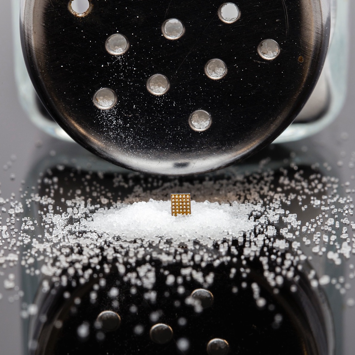
Lattice Semiconductor revels in being the holder of the “World’s Smallest FPGAs” title. While Xilinx and Intel/Altera boast about gazillions of LUTs, scores of DSP blocks, and multi-gigabit SerDes packed into silicon platforms that you could probably land a small helicopter on, Lattice attacks the opposite end of the spectrum – FPGAs so small you could sneeze and knock a dozen off your lab bench by accident.
Five years ago, Lattice acquired the iCE family along with FPGA startup SiliconBlue, who specialized in tiny, one-time-programmable, microwatt-sipping FPGAs, targeted at the high-volume consumer market. The company had numerous design wins in mobile phones, tablets, and other battery-powered portable devices where just a little programmable logic could be a game changer. Since the acquisition, iCE has become an increasingly large portion of Lattice’s strategy, as the company has refined and upgraded the line to attract ever larger and more sophisticated segments of the market.
Now, the company is rolling out their new “iCE40 UltraPlus” family, which boasts some good stuff that should open some new opportunities for the world’s smallest FPGAs. And, yeah, the name “UltraPlus” shows the danger of throwing an “Ultra” onto your product name. I mean, where do you go from there? Four years from now will we have SuperBeyondUltraDoublePlus2? But, naming issues aside, UltraPlus is designed to elevate the tiny devices from connectivity and glue logic roles to computation. In fact, Lattice refers to UltraPlus devices as “mobile heterogeneous computing (MHC) solutions.”
What makes iCE40 UltraPlus live up to the MHC moniker? Lattice has added resources that beef up the chip for computation – by giving it eight times the memory of previous versions (1.1Mbits of RAM), 8 DSP blocks, up to 5K LUTs, MIPI-I3C support, and under 100 microwatts of standby power consumption. The idea is to give your mobile device a lot of computing and sensor aggregation capability even when your application processors are taking a nap. The iCE40 device can be buffering sensor data and doing preliminary analysis and data reduction for activities like gesture recognition, facial recognition, audio enhancement, and so forth.
Lattice’s concept for UltraPlus is solid. In edge IoT devices, there is a need for always-on, always-sensing operation. In many cases, power is at a premium. That means we need something like a tiny, capable, FPGA sitting near the IOs that can do tasks like sensor data buffering, sensor fusion and aggregation, and even monitoring of low-resolution, always-on camera video streams – all while the main, power-hungry applications processors are powered down. Then, when the FPGA figures out that something important is going on, it can call in reinforcements – wake up the applications processors, release the dogs, and sound the alarm.
In many designs, microcontrollers (MCUs) are used for similar tasks. But an FPGA like iCE40 UltraPlus can outperform an MCU in just about every dimension. The FPGA fabric can do simple functions in hardware that would require much more power and latency in an MCU. The FPGA can be configured to handle just about any type of IO that your system can throw at it. The FPGA can be set up to consume significantly less power, particularly taking advantage of stand-by modes and tasks that require no complex software at all.
In wearable devices, there is often a need for a device that can keep the display alive with a large, low-power frame buffer while also acting as an interface bridge. In sensor fusion applications, there is a need for a device to buffer, aggregate, and do as much filtering and processing of incoming data as possible without awakening the applications processor. In audio applications, a device is needed to do complex beamforming from an array of microphones to reject noise and identify specific voices or sound sources. UltraPlus is designed and sized to perform these types of functions in IoT edge devices.
Unlike conventional FPGAs, iCE40 devices are one-time programmable (OTP) and have configuration data built in via non-volatile configuration memory. That means you don’t need additional configuration circuitry to support the FPGA at startup, and the device can boot practically instantly.
The iCE40 series is comprised of three families: iCE40 UltraLite, iCE40 Ultra, and iCE40 UltraPlus. The new UltraPlus includes two device sizes/densities – 2800 and 5280 LUTs with four or eight DSP blocks, and 80Kb or 120Kb block RAM respectively. An additional 1Mb of RAM is delivered via four 256K single-port memory blocks. Hardened IOs include I2C, I3C, VGIO, SPI, and MIPI-DPHY, and the two devices include 21 or 39 GPIOs respectively.
iCE40 UltraPlus is available in two packages – 2.15mm x 2.55mm CSP with 0.4mm pitch. (Nope, not a typo. They aren’t kidding about this “World’s Smallest FPGA” stuff.) And if you prefer 0.5mm pitch, a palatial 7mm x 7mm QFN. For an instant-on, single-chip FPGA for IO bridging, sensor fusion, and compute acceleration, this provides a flexible, nicely integrated package with a tiny footprint and minimal impact on your PCB design.
For everything from wearables and medical devices to drones and white goods, iCE40 UltraPlus could be a real enabler, solving the ongoing battle between power consumption and computing power required as we bring up sensor-laden IoT edge devices in large volumes. Lattice seems to have locked into a solid segment with this high-volume, consumer-oriented focus, and it clearly separates them from the traditional FPGA pack. It’ll be interesting to see the range of applications that iCE40 UltraPlus enables over the next couple of years.


